
Design for Testability DFT for PCB Basics and Test Strategy

Table of Contents
Highleap Electronics provides PCB fabrication and PCB assembly, and we check testability during our free DFM review. The goal is simple: fewer surprises during build, clearer pass fail results, and faster delivery.
DFT PCB Basics
Design for Testability DFT means designing your PCB so manufacturing can verify it efficiently. It is not a “nice to have” feature. It directly impacts:
- Delivery time because boards that are hard to test require more manual probing and longer debug loops
- Yield because untestable nets let defects escape until later stages
- Cost because repeated rework and engineering time quickly exceed the cost of adding test access
- Consistency because clear test access enables repeatable testing across batches and factories
Most assembly defects are not mysterious. They are typically opens, shorts, solder faults, polarity issues, wrong values, or missing parts. DFT ensures the factory can detect and isolate those defects quickly.
PCBA Test Strategy
Good DFT starts with choosing a realistic test strategy. You do not need every method. You need the right combination for your volume, density, and risk.
In circuit test ICT
- Best for medium and high volume where fast cycle time and repeatability matter
- Strength excellent coverage of manufacturing defects when access exists
- Requirement sufficient test points and usually a fixture
Flying probe test
- Best for prototypes and low volume where design changes are frequent
- Strength no fixture investment and flexible for revisions
- Tradeoff slower per board than ICT
Boundary scan JTAG
- Best for dense digital designs with JTAG capable devices
- Strength adds coverage without needing probe pads for every net
- Limit does not replace analog checks or full functional verification
Functional test
- Best for verifying the product works under power and real conditions
- Strength validates design intent
- Risk can miss assembly defects if coverage is not planned
Typical real world mix is Flying Probe plus Functional for prototypes, and ICT plus Functional for production. If ICT is not feasible, a planned mix of selective probing, JTAG where available, and functional test can still achieve strong confidence.
PCB Test Point Design
Test points are the highest ROI DFT feature. If your test points are easy to access, production test becomes fast and repeatable. If they are missing or poorly placed, testing becomes manual, slower, and less consistent.
Test point size and finish
- Flying probe commonly works well with dedicated pads around 0.5mm to 0.7mm diameter, depending on your density and probe system
- ICT fixtures typically prefer larger dedicated pads around 0.9mm to 1.0mm diameter for reliable contact and lower false failure rate
- Surface finish should be probe friendly and stable. Avoid relying on solder coated pads for probing because it can increase variability. Dedicated exposed copper pads with proper finish are more consistent.
Practical advice If you are unsure which test method will be used, design test points that are at least flying probe friendly, then reserve open areas that could support ICT in a future production revision.
Test point spacing and access
Test points fail most often because probes cannot physically reach them. Common access rules:
- Keepouts leave clearance from tall components, shields, connectors, and heatsinks so probes do not collide
- Board edge margin avoid placing test points too close to the PCB outline where fixtures and clamps may interfere
- Single side probing if possible, keep the majority of test points on one side to simplify test setup and reduce cost
If your board must be tested from one side, prioritize critical nets on that side first, then place secondary nets where space allows.
Which nets should get test points
In production, you rarely need a test point on every net. You need coverage on the nets that quickly reveal assembly defects and isolate failures.
- All power rails each voltage domain should have accessible measurement points
- Multiple grounds stable ground access reduces noise and false failures during measurement
- Programming and debug access SWD JTAG UART or programming headers prevent stalled builds when firmware or configuration is needed
- Reset enable clocks basic control nets that determine whether the board is alive
- Key analog nodes sense lines references and feedback points where you can define pass fail thresholds
- Interfaces key pins for communication ports used for functional testing
High yield principle Add test points where a measurement can confirm multiple things at once, such as a rail that also validates a regulator, a sense network, and a downstream load condition.
How to label and document test points
Even perfect test points lose value if they are hard to identify. To avoid slow debug during production:
- Name test points with clear identifiers such as TP1 TP2 plus net name in documentation
- Include a test point list in your assembly package mapping TP to net name and expected values
- Provide an assembly view showing locations for quick operator reference
Test points and high speed signals
High speed nets and controlled impedance traces require special care. A poorly placed test pad can create stubs and degrade signal integrity.
- Avoid test pads on controlled impedance lines when possible
- Use the smallest feasible pad and keep the stub as short as possible if probing is required
- Prefer connector based access for some high speed interfaces where probing is not practical
If you must probe a high speed net, document the measurement method and acceptable limits so the test is consistent and does not create false failures.
Quick test point checklist
- Dedicated test pads are used for critical nets rather than relying on vias
- Test points are accessible and not blocked by tall parts or shields
- Power and ground points are sufficient for stable measurement
- Programming and debug access is included
- Documentation clearly maps TP identifiers to nets and expected values
When these items are in place, production testing becomes faster, and failures become easier to diagnose. That typically reduces rework time and improves delivery predictability.
ICT Design Guidelines
ICT is often the fastest production test method, but only if the PCB supports it. If your product volume is growing, designing with ICT in mind can pay back quickly.
- Probe access planning ensure the critical nets are reachable without collisions and that test points are not hidden under components
- Grounding strategy provide multiple ground probe points to lower impedance and improve measurement stability
- Board support plan mechanical support areas so probe pressure does not flex the PCB and cause intermittent contact or damage
- Coverage priority focus ICT access on power, reset, references, and failure isolating nodes rather than trying to access everything
If your PCB is too dense for broad ICT, a hybrid strategy can still be production friendly. Flying probe or selective ICT coverage plus functional testing often achieves strong results without forcing an unrealistic layout.
DFT Review at Highleap
Highleap Electronics is a PCB manufacturing and PCB assembly factory. Our goal is not to teach theory. Our goal is to ship boards that pass test quickly and consistently. That is why we review testability as part of our free DFM review.
What we check before production
- Test point access and feasibility for ICT or flying probe
- Programming and debug access readiness
- JTAG chain access and documentation when applicable
- Functional test inputs needed to define pass fail criteria
- Practical suggestions to reduce test time and improve isolation
What to send for the fastest review
- Gerber or ODB plus drill files
- BOM and centroid CPL file
- Your volume estimate prototype or production
- Any no substitution or compliance constraints
- Functional expectations or a basic test checklist if you have one
Request Free DFM and DFT Review
DFT is easiest to fix before a build starts. If you want smoother testing and fewer delays, send your files and we will tell you what to change and what can stay as is.

Charles has over 10 years of experience in PCB CAM engineering and electronics manufacturing, specializing in PCB file verification, DFM analysis, and production preparation for multilayer, HDI, RF, and high-speed boards. Proficient in Genesis, InCAM, and CAM350, he ensures accurate data, stable processes, and high manufacturing yield.
At Highleap Electronics, he focuses on process optimization and manufacturability evaluation to help customers reduce risks, shorten lead times, and achieve reliable production results.

Recommended Posts

TUC TU-872 SLK PCB for High-Speed FR-4 Cost Control
TUC TU-872 SLK occupies a commercially useful middle...

Shengyi S1000-2M PCB for Thick Multilayer Reliability
Shengyi S1000-2M is a high-Tg, low-CTE FR-4.0 laminate for...
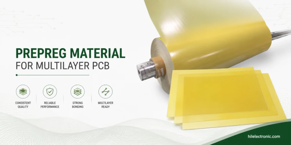
Isola P25N PCB for No-Flow Bonding and Cavity Builds
Isola P25N is a polyimide UL HB No-Flo® specialty prepreg....
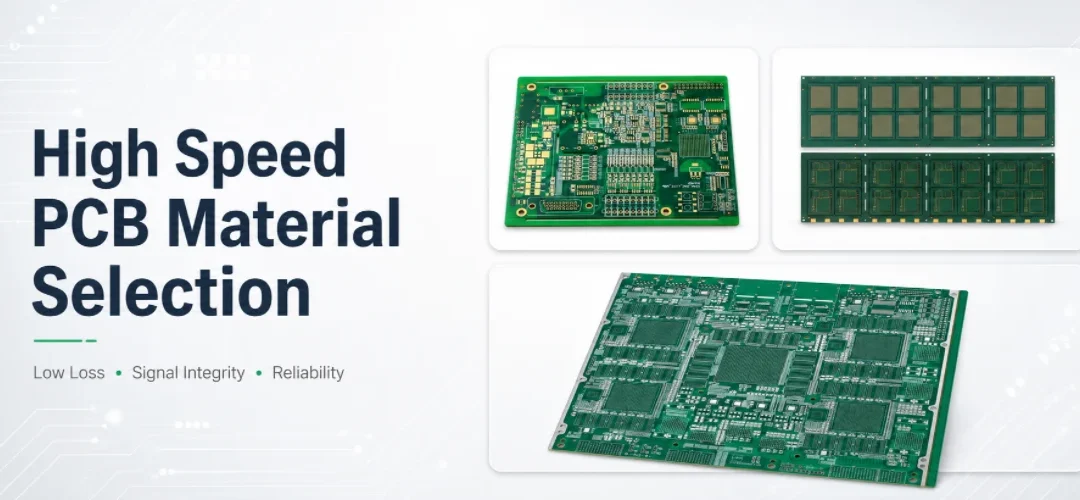
ITEQ IT-88GMW PCB for 77 GHz Radar Modules
A 76–81 GHz automotive radar PCB is an electromagnetic...
How to get a quote for PCBs
Let us run DFM/DFA analysis for you and get back to you with a report.
You can upload your files securely through our website.
We require the following information in order to give you a quote:
-
- Gerber, ODB++, or .pcb, spec.
- BOM list if you require assembly
- Quantity
- Turn time
In addition to PCB manufacturing, we offer a comprehensive range of electronic services, including PCB design, PCBA (Printed Circuit Board Assembly), and turnkey solutions. Whether you need help with prototyping, design verification, component sourcing, or mass production, we provide end-to-end support to ensure your project’s success. For PCBA services, please provide your BOM (Bill of Materials) and any specific assembly instructions. We also offer DFM/DFA analysis to optimize your designs for manufacturability and assembly, ensuring a smooth production process.