
HDI Blind Via PCB Cost Drivers Lamination Drill and Design

Table of Contents
HDI blind via PCB cost is driven by process complexity, not materials. Sequential lamination cycles, laser drilling setup, and via filling requirements dominate the cost structure — not board area or copper weight. A Type I HDI board (1+N+1) runs 2.3–3.2× a comparable through-hole design. Type II (2+N+2) adds another 1.7–2.1× on top of that. Type III and any-layer HDI reach 4–8× standard PCB costs.
Understanding which HDI features your design actually requires — and which are over-specified — is what separates a cost-optimized HDI program from one that pays a 40–60% premium for no electrical benefit.
Get HDI Blind Via Cost Analysis
1) HDI Blind Via PCB Cost Drivers
On a standard PCB, materials and basic processing account for most of the cost. On an HDI board, lamination cycles and drilling complexity take over. This shift has a direct implication: optimizing HDI cost means reducing lamination cycles and via count — not negotiating on laminate price.
Cost Structure: Standard PCB vs. HDI
| Cost Component | Standard 6L | Type I HDI (1+4+1) | Type II HDI (2+2+2) |
|---|---|---|---|
| Base materials | 20–30% | 15–22% | 12–18% |
| Lamination | 8–12% | 12–18% | 18–25% |
| Drilling (all types) | 8–12% | 18–28% | 25–35% |
| Testing & inspection | 5–8% | 8–12% | 10–15% |
| Yield loss allocation | 3–5% | 6–10% | 8–14% |
Concrete Cost Example: 100×100 mm 6-Layer Board at 100 Pieces
- Standard 6L (through-hole): $12–18/board
- Type I HDI (1+4+1): $32–48/board — the $20–30 premium comes from two lamination cycles, laser drilling setup, and X-ray inspection, not from materials
- Type II HDI (2+2+2): $55–82/board — the additional $23–34 over Type I comes from a third lamination cycle, second laser drilling operation, and via filling
Each HDI complexity step carries a similar absolute cost increment. The question is always whether the routing benefit justifies it.
Why HDI Cost Doesn’t Scale with Board Area
Standard PCB cost correlates with board area. HDI cost correlates with via count and lamination cycles. A 50×50 mm Type I board with 400 microvias often costs as much as a 150×150 mm Type I board with 200 microvias — the smaller board has twice the via density, not half the cost.
2) 1+N+1 vs. 2+N+2 vs. Any-Layer: Cost Progression
Type I (1+N+1): Entry-Level HDI
One buildup layer added to each outer surface of a standard multilayer core. Blind vias connect L1–L2 and Ln–Ln-1. Through-holes still penetrate the full stackup.
Cost drivers: one additional lamination cycle, laser drilling setup, X-ray inspection for blind via quality, tighter registration (±0.075 mm vs. ±0.15 mm standard).
Typical cost multiple: 2.3–3.2× comparable through-hole design.
Justified when: 0.40–0.50 mm pitch BGA requiring via-in-pad or near-pad routing; board size reduction of 20–30% vs. through-hole; RF designs where through-hole via stubs degrade performance above 5 GHz.
Type II (2+N+2): Dual Buildup
Two sequential buildup layers on each outer surface. Enables two levels of blind vias: first buildup creates L1–L2 blind vias; second buildup creates L1–L3 connections via stacked or staggered microvias, mirrored on the bottom surface.
Cost drivers: two additional lamination cycles, two laser drilling operations, via filling if stacked vias are used ($0.05–0.15 per via for resin plug, $0.20–0.50 for copper fill).
Typical cost multiple: 4.2–6.5× through-hole, or 1.7–2.1× Type I.
Justified when: 0.30–0.40 mm pitch BGA with high I/O; board size reduction of 35–50%; layer count reduction (8-layer Type II may replace a 10-layer through-hole design).
Type III: Buried Vias Plus Buildup
Inner layer cores with buried vias, plus buildup layers with blind vias on outer surfaces.
Cost drivers: 4–5 lamination cycles, multiple laser and mechanical drilling operations, higher yield loss allocation (more process steps = more defect opportunities).
Typical cost multiple: 5.8–9.5× through-hole, or 1.35–1.85× Type II.
Justified when: 12–20 layer boards where buried vias reduce total layer count by 20–30%; high-speed digital designs requiring layer transitions without via stubs.
Any-Layer HDI (Type IV–VI)
Sequential buildup from core outward, any layer connectable to any other through stacked and staggered microvias. 5–8 lamination cycles; laser drilling after each lamination; planarization at every buildup stage.
Typical cost multiple: 8–16× through-hole.
Justified when: Smartphone and tablet main boards, advanced IC package substrates, or applications where board cost is negligible relative to component or system value.
3) Laser vs. Mechanical Drilling Economics
Laser Drilling Cost Breakdown
Laser drilling (CO₂ or UV) is required for microvias <0.20 mm diameter.
| Cost Element | Per Panel | Per Via (500 vias/panel) |
|---|---|---|
| Setup (alignment, program load) | $100–200 | $0.20–0.40 |
| Drilling time | $15–30 | $0.03–0.06 |
| Equipment amortization + consumables | $28–55 | $0.06–0.11 |
| Total | $143–285 | $0.29–0.57 |
Setup cost dominates at low via counts. For panels with <100 vias, setup runs $1–2 per via. At 1,000+ vias per panel, setup drops to $0.10–0.20 per via.
Mechanical Drilling Cost Breakdown
Mechanical drilling is viable for blind vias ≥0.20 mm diameter with aspect ratio ≤5:1.
| Cost Element | Per Panel | Per Via (500 vias/panel) |
|---|---|---|
| Setup | $25–50 | $0.05–0.10 |
| Drilling time + tool wear | $20–42 | $0.04–0.09 |
| Equipment amortization | $6–12 | $0.01–0.02 |
| Total | $51–104 | $0.10–0.21 |
For vias ≥0.20 mm, mechanical drilling costs 50–65% less per via than laser.
Hybrid Drilling: The Practical Cost Optimization
Most boards benefit from combining both methods. Laser drill fine-pitch BGA areas and vias <0.20 mm; mechanically drill power, ground, and thermal vias ≥0.20 mm in lower-density regions.
Example: Type I HDI with 600 blind vias
- All laser: 600 × $0.35 = $210/board
- Hybrid (200 laser + 400 mechanical): $70 + $48 = $118/board
- Saving: $92/board (44%). At 500 boards: $46,000.
4) Via Filling and Stacking Cost Impact
Via Fill Method Comparison
| Fill Method | Cost per Via | Required For |
|---|---|---|
| Unfilled | $0 (baseline) | Non-stacked, non-via-in-pad |
| Resin plug | $0.05–0.15 | Single-level stacked vias, some via-in-pad |
| Copper fill (electroplating) | $0.20–0.50 | Via-in-pad under fine-pitch BGA, multi-level stacking |
| Copper fill + planarization | $0.30–0.70 | Via-in-pad with tight coplanarity requirements |
| Conductive paste | $0.08–0.22 | Cost-sensitive consumer products with relaxed reliability |
Stacked vs. Staggered Microvias
This is the single highest-impact cost decision in Type II and Type III HDI design.
Stacked microvias align vias on consecutive buildup layers at the same X-Y position. They require fill and planarization before the next lamination — adding $0.30–0.70 per stacked via pair plus X-ray inspection.
Staggered microvias offset vias by ≥0.25 mm between layers, connected by short traces on intermediate layers. No fill is required. No additional processing cost beyond the baseline blind via.
Example: Type II HDI with 300 inter-layer connections
- Stacked: 300 pairs × $0.50 = $150/board
- Staggered: $0 additional
- Saving: $150/board. At 500 boards: $75,000.
- Trade-off: staggered requires ~5–8% more routing area. Worthwhile unless density is absolutely maximized.
Via-in-Pad (VIP) Costs
Via-in-pad places vias directly inside component pads — the only routing solution for 0.30–0.35 mm pitch BGAs, and sometimes necessary for 0.40 mm pitch with high I/O count.
Cost impact: copper fill + planarization $0.30–0.70 per via; additional X-ray inspection $3–8 per panel; higher assembly yield loss allocation (VIP increases defect risk by 2–4%).
Cost optimization: Use dog-bone vias (offset 0.20–0.30 mm outside the pad) wherever pitch allows. Dog-bone eliminates fill requirements entirely, saving $0.25–0.60 per via. For more on via-in-pad implementation in flex and rigid-flex HDI designs, the same cost logic applies with additional material considerations.

5) Design Decisions That Control Cost
HDI Type Selection: Use the Minimum Required
HDI types are not quality grades. Type I is not inferior to Type II — it is the correct choice when Type I meets your routing requirements. Over-specifying HDI type is the most common and most expensive design mistake.
| Application | Minimum HDI Required | Common Over-Spec | Cost of Over-Spec |
|---|---|---|---|
| 0.50 mm pitch BGA (256 I/O) | Standard through-hole (dog-bone) | Type I “for future flexibility” | +$18–28/board (+135–180%) |
| 0.40 mm pitch BGA (484 I/O) | Type I (blind vias around perimeter) | Type II “for better routing” | +$22–35/board (+65–95%) |
| 0.30 mm pitch BGA (676 I/O) | Type II (2 buildup layers required) | Type III “for premium feel” | +$28–48/board (+45–75%) |
Via Diameter Standardization
Designs that specify 3 or more via diameters (0.10, 0.15, 0.20 mm) force multiple laser parameter changes or drill bit swaps, adding setup time per diameter change.
Standardize on two diameters maximum: 0.15 mm for highest-density BGA regions; 0.20 mm for everything else (which also enables mechanical drilling in lower-density areas). Typical saving: 8–15% of via drilling cost.
Panel Utilization
HDI drilling cost is charged per panel, not per board. A 2–3 mm dimension change that improves panel utilization by 10–15% translates directly to per-board cost reduction.
Example: Changing from 82×118 mm (20 boards/panel) to 80×115 mm (24 boards/panel) at 350 vias/board:
- Current: $38/board
- Optimized: $32/board (20% utilization gain → 16% cost reduction)
Layer Count Reduction Through HDI
HDI enables higher routing density per layer, potentially reducing total layer count. An 8-layer standard through-hole board may be achievable as a 6-layer Type I HDI — saving 2 inner layers in material and processing.
The comparison: 8L standard = $18, 6L Type I = $32. HDI costs more per board but enables a smaller footprint. If board area shrinks 25% due to HDI density, effective cost becomes $32 × 0.75 = $24 — cheaper than the 8L through-hole design while delivering better signal integrity.
6) Volume Economics and NRE Amortization
NRE Cost Breakdown by HDI Type
| NRE Component | Type I | Type II | Type III |
|---|---|---|---|
| Stackup design & simulation | $180–400 | $300–600 | $450–900 |
| Photo-tooling (all layers) | $120–280 | $150–320 | $200–420 |
| Laser drilling program | $150–350 | $250–500 | $350–650 |
| Test fixture + first article | $230–530 | $300–670 | $420–930 |
| Total NRE | $730–1,680 | $1,060–2,240 | $1,500–3,100 |
NRE Amortization at Different Volumes
Type I HDI example (NRE = $1,200, base cost = $35/board):
- 10 boards (prototype): NRE adds $120/board → $155 total
- 50 boards: NRE adds $24/board → $59 total
- 100 boards: NRE adds $12/board → $47 total
- 500 boards: NRE adds $2.40/board → $37.40 total
- 2,000 boards: NRE adds $0.60/board → $35.60 total (essentially at base cost)
Prototype HDI pricing is 3–4× production pricing purely because of NRE amortization. Never extrapolate prototype unit cost to forecast production budgets.
Volume Pricing Structure
| Quantity | Primary Cost Reduction Mechanism | Typical Reduction vs. Prototype |
|---|---|---|
| 10–25 (prototype) | NRE fully loaded, minimum order quantities | Baseline |
| 50–100 (pilot) | NRE amortization begins, full panel utilization | −35% to −50% |
| 100–500 (production) | NRE negligible, material volume pricing | −55% to −68% |
| 500–2,000 | Bulk material procurement, dedicated tooling | −65% to −78% |
| 2,000+ | Annual agreements, consignment material | −70% to −82% |
7) Cost-Optimized HDI Solutions from Highleap
Highleap Electronics fabricates HDI blind via PCBs from Type I through Type III, including stacked microvia structures, complex HDI stackup configurations, and hybrid builds with Rogers or Megtron outer layers on FR4 inner cores.
Transparent Cost Breakdown
Every Highleap HDI quote itemizes costs separately:
- Base materials by laminate type and copper foil grade
- Lamination cycles (typically $2.50–4.00 per cycle per board)
- Laser drilling setup + per-via cost, and mechanical drilling, shown separately
- Via filling (resin plug vs. copper fill, cost per via)
- Testing: standard (visual + electrical + sample X-ray) vs. enhanced (100% X-ray) vs. Class 3 (micro-section)
- NRE shown separately with 24-month tooling retention
DFM Cost Reduction Review
Highleap engineering reviews every new HDI design before quoting. Typical findings:
- HDI type reduction: Evaluate whether a Type II design can route as Type I through layer reassignment — typical saving $22–35/board
- Fill elimination: Flag vias specified as filled that don’t require filling (not via-in-pad, not stacked) — saving $0.05–0.15 per via
- Hybrid drilling conversion: Flag vias ≥0.20 mm eligible for mechanical drilling — saving $0.15–0.25 per via
- Stacked-to-staggered: Suggest staggered routing alternatives — saving $0.30–0.70 per via pair
- Panel optimization: Recommend 1–3 mm dimension adjustments that improve panel utilization 10–25%
These recommendations are returned within 8–12 hours at no charge and typically identify 15–35% cost reduction without design re-spin. For an overview of what information is needed to get an accurate HDI blind via PCB quote, see our quoting guide.
Volume Pricing
| Quantity | Type I Unit Price | Type II Unit Price | Additional Benefits |
|---|---|---|---|
| 10 (prototype) | $65–95 | $110–155 | Free DFM + stackup optimization |
| 50 | $42–58 | $72–98 | Tooling retained 24 months |
| 100 | $35–48 | $58–78 | Priority scheduling |
| 500 | $28–38 | $48–65 | Material volume pricing |
| 2,000 | $24–32 | $42–55 | Blanket PO, consignment material option |
Process Capability and Yield
- Type I HDI first-pass yield: 97–98% (industry average 94–96%)
- Type II HDI first-pass yield: 95–97% (industry average 90–94%)
- Blind via open rate: <0.5% (industry average 1.5–3% on first production run)
- Registration accuracy: ±0.060 mm typical, ±0.085 mm maximum
Higher yield reduces total cost of ownership beyond the quoted price — fewer boards rejected at incoming inspection, fewer assembly failures traced to substrate defects.
For designs combining HDI with advanced RF requirements, Highleap also fabricates hybrid HDI/high-frequency stackups using Rogers and Megtron laminates on HDI cores. For complex HDI applications in compact platforms, see our drone and UAV HDI PCB and semiconductor packaging HDI guides for application-specific design considerations.
Get Your Cost-Optimized HDI Quote
Frequently Asked Questions
What is the biggest cost driver in HDI blind via PCB manufacturing?
Sequential lamination cycles and laser drilling setup — not materials. On a standard PCB, base materials represent 20–30% of cost. On a Type II HDI board, drilling alone accounts for 25–35% and lamination 18–25%, while materials drop to 12–18%. This is why cost optimization focuses on reducing lamination cycles and via count, not on negotiating laminate price.
How much more does Type II HDI cost compared to Type I?
Type II (2+N+2) runs 1.7–2.1× the cost of an equivalent Type I (1+N+1) board. For a 100×100 mm 6-layer board at 100 pieces, Type I costs $32–48/board and Type II costs $55–82/board. The additional cost comes from a third lamination cycle, a second laser drilling operation, and via filling requirements — not from the substrate material itself.
When is via filling actually required on an HDI blind via PCB?
Via filling is only structurally required in two situations: via-in-pad locations under fine-pitch BGA pads (to prevent solder wicking during assembly), and stacked microvia configurations where a via on one buildup layer sits directly above a via on the previous layer. Vias that are neither via-in-pad nor stacked do not require filling. Specifying copper fill on unfilled-eligible vias adds $0.20–0.50 per via unnecessarily — one of the most common over-specification errors in HDI design.
Why is prototype HDI pricing so much higher than production pricing?
NRE (non-recurring engineering) costs are fully loaded onto prototype quantities. For a Type I HDI board, NRE totals $730–1,680 — spread across 10 prototype boards, that adds $73–168 per board. At 500 production boards, the same NRE adds only $1.46–3.36 per board. Prototype HDI pricing is typically 3–4× production pricing for this reason alone. Never use prototype unit cost to estimate production program budgets.
What is the most cost-effective way to reduce HDI blind via PCB cost without a redesign?
Three changes deliver the highest savings without touching the schematic or layout: (1) Switch from all-laser to hybrid drilling — vias ≥0.20 mm drilled mechanically cost 50–65% less per via than laser-drilled; on a 600-via board this saves ~$92/board. (2) Convert stacked microvias to staggered — eliminates $0.30–0.70 per via pair in fill and planarization cost. (3) Adjust board dimensions by 1–3 mm to improve panel utilization by 10–25%, which reduces per-board cost proportionally since laser drilling is charged per panel.
Does a higher HDI type always mean better electrical performance?
No. HDI type is a manufacturing complexity classification, not a quality grade. Type I is not electrically inferior to Type II when Type I meets the routing requirements. Specifying Type II for a 0.40 mm pitch BGA that could route as Type I adds $22–35/board with no electrical benefit. The correct HDI type is the minimum that satisfies your actual via density, pitch, and layer transition requirements — determined by routing analysis, not by product tier.

Recommended Posts
LED Parking Lot Light PCB Manufacturing & Assembly by Highleap Electronics
Figure 1. LED parking lot light PCB production and...
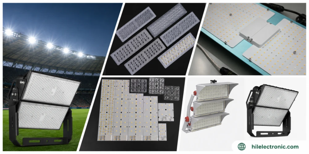
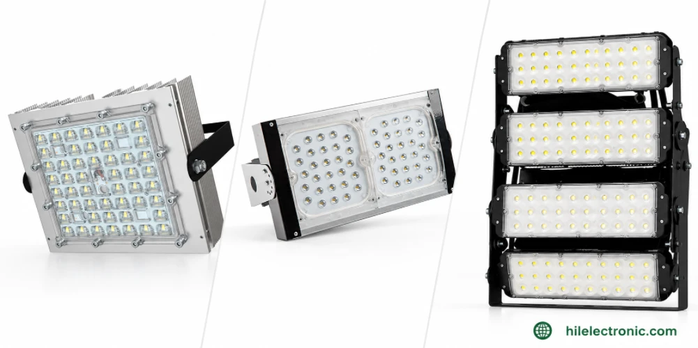
LED Stadium Light PCB Manufacturing — Very-High-Power Engines & Flicker-Free Drivers
Figure 1. LED stadium light PCB production and assembly...
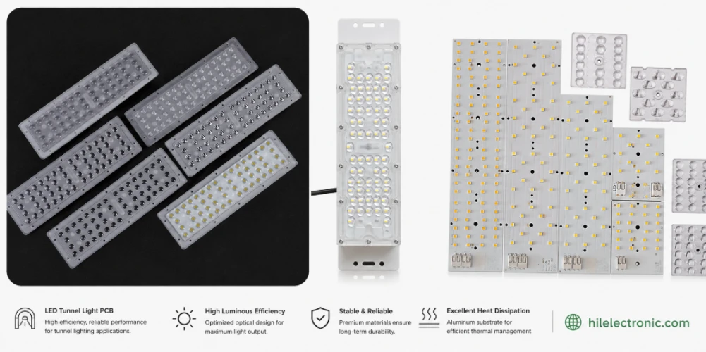
LED Tunnel Light PCB Manufacturing — High-Reliability Engines & Drivers
Figure 1. LED tunnel light PCB production and assembly...
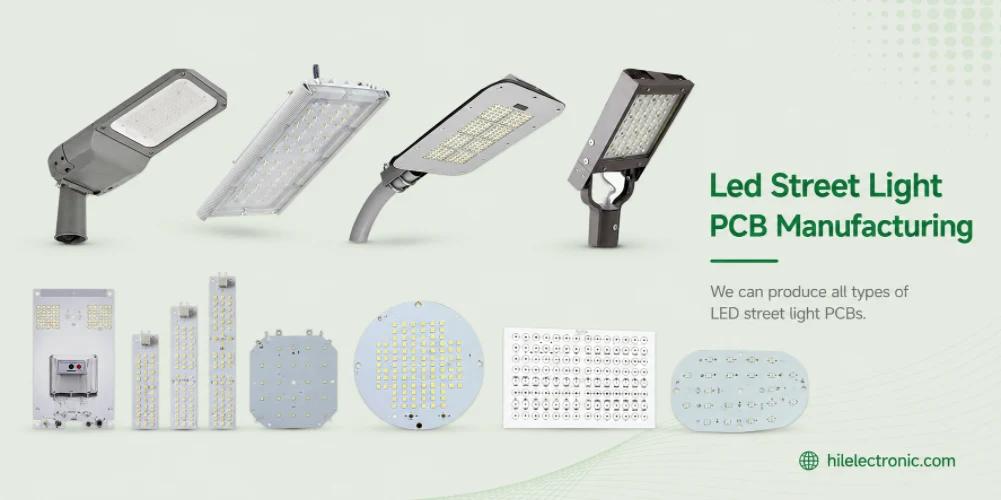
LED Street Light PCB Manufacturing & Assembly by Highleap Electronics
Figure 1. LED street light PCB production and assembly...
How to get a quote for PCBs
Let us run DFM/DFA analysis for you and get back to you with a report.
You can upload your files securely through our website.
We require the following information in order to give you a quote:
-
- Gerber, ODB++, or .pcb, spec.
- BOM list if you require assembly
- Quantity
- Turn time