
Reliable HDI Flex PCB Manufacturer | Highleap Electronic

HDI Flex PCB
For over a decade, Highleap Electronics has been a leader in next-generation µVia technologies. As traditional laser via plating approaches its limits, our HDI flex PCBs are driving the future of electrical performance and reliability. By utilizing µVia as small as 50 μm and copper as thin as 8 μm, we are pushing the boundaries of density in compact electronic packages.
At the forefront of FPC (Flexible Printed Circuit) technology, Highleap Electronics enables the miniaturization of 3D devices with very low bending radii and Ultra-HDI capabilities. This breakthrough allows the creation of smaller, highly integrated wearables and high-density signal applications.
With a proven track record in flex circuits, we offer products with layer counts from 1 to 16, working with ultra-thin polyimide foils (as thin as 12.5 µm) and precision adhesive bond plys. Our laser-drilled vias as small as 35 µm in diameter can be filled with copper to create advanced via-in-pad structures, ensuring high reliability and repeatability in every product.
Benefits of HDI Flex PCBs
High-Density Interconnect (HDI) flexible circuits offer a range of advantages over typical flexible circuits, including:
1. Lower Cost and Smaller Size: Increased circuit density can eliminate extra layers, saving up to 40% compared to non-HDI designs.
2. Advanced Component Packaging: HDI allows for high-I/O and fine-pitch feature capabilities.
3. More Design Options and Flexibility: Blind and buried microvias allow for conductor routing on internal layers under vias, creating more usable design space per layer.
4. Improved Electrical Performance and Signal Integrity: Microvias in high-speed circuits improve electrical performance by allowing shorter circuit paths, stub reduction, and lower crosstalk and noise.
5. Improved Thermal Performance and Reliability: Microvias lower the z-axis thermal stresses between adjacent layers.
6. Improved Cost Effectiveness: Highleap Electronic’s 18” x 24” (45.7 cm x 61 cm) panel size maximizes panel density, increasing the efficiency of the assembly process.
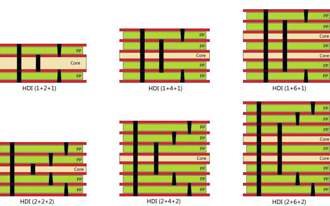
HDI Flex PCB Capability Overview
At Highleap Electronics, our HDI Flex PCB technology is engineered for high-density, compact designs with exceptional performance. We offer flexible PCBs ranging from 3 to 16 layers, designed to meet the needs of modern electronics.
Our HDI Flex PCBs feature microvia sizes as small as 50 μm finished, with fine line and spacing at 50 μm. Advanced sequential build technology allows for reliable blind and buried vias, while copper via fill ensures long-term durability. See the table below for a detailed overview of our HDI Flex PCB capabilities, optimized for high-performance applications.
| Capability | Specification |
|---|---|
| Layer Count | 3-16 layers |
| Minimum Microvia Size | 75 μm, 50 μm finished |
| Minimum Microvia Pad Size | Via diameter + 150 μm |
| Minimum Line and Spacing | 50 μm |
| Microvia Blind Plating Aspect Ratio | 1:1 (depth to diameter) |
| Minimum Core Dielectric Thickness | 25 μm |
| Minimum Copper Thickness | 9 μm |
| Blind & Buried Via Construction | Sequential build technology |
| Via Fill | Copper via fill available |
Materials Used in HDI Flex PCBs
The materials used in HDI Flex PCBs are carefully selected to ensure high performance and reliability in various applications. Below is an overview of the key materials used in the manufacturing process:
- Cover/Substrate
- Polyimide Film: Available in thicknesses of ½ mil (12μm), 1 mil (25μm), 2 mil (50μm), 3 mil (75μm), and 5 mil (125μm)
- Liquid Photoimageable Coverlay (LPI): Used for precise and durable surface protection.
- Conductor
- Copper: Offered in various thicknesses: 1/8 oz. (5μm), 1/4 oz. (9μm), 1/3 oz. (12μm), 1/2 oz. (18μm), 1 oz. (35μm), 2 oz. (71μm), 3 oz. (107μm)
- Stiffener
- Epoxy-Glass (FR-4), Polyimide-Glass, Polyimide, Copper, Aluminum: Used to enhance structural integrity and support flexibility.
Technological Highlights of HDI Flex PCBs

- Turnkey flex solutions targeting 3D miniaturization
- Highly reliable, extremely robust multilayer flex/microvia substrates
- Ultra-thin base materials
- Filled via and stacked via process available
- Complex mechanical/assembly assist features, including special profiles, fold lines, cut-outs, and thinned bending zones/cavities
- Wrap-around boards
- Chip-on-flex (COF), chip-scale packaging (CSP) substrates, and BGAs
- A wide variety of surface finishes, including OSP, ENIG, ENEPIG, E-AU, and DIG
- Flying leads
- Bending test for flexible circuits
- Ultra-fine line flex cables
Why Use Blind Via Flex PCBs
In modern flex PCB designs, high-density components—similar to those found in rigid PCBs—are often required. To accommodate these components, blind and/or buried vias are essential for routing signal lines effectively within the design. One of the most common drivers for this need is the 0.4mm pitch BGA package.
Blind vias allow signals to be routed from the BGA SMT pad to the next layer and then outwards. In high pin count devices, additional blind and buried vias are often necessary to ensure proper signal routing and reliable performance.
However, implementing these vias in flex PCB designs presents unique challenges compared to rigid PCBs, due to differences in materials and manufacturing processes. The flexibility of the substrate, along with the precise drilling and plating techniques required, makes designing blind via flex PCBs a more specialized process.
The Role of Via-in-Pad in High-Layer Count Flex PCB Designs
For flexible PCB designs with high layer counts utilizing high-density outer layers, the extra area used for separate pads and SMT components limits the available space for trace fan-out. Designing via-in-pad in flex and rigid-flex PCBs can significantly increase density by utilizing vias as mounting pads. The copper- or silver-filled flat vias allow for soldering components directly on via holes.
Although via-in-pad technology can release extra surface area for routing traces, there are a few points to be aware of when using this type of construction with flex. Manufacturers typically fill rigid PCB vias for SMT pads with a conductive epoxy, copper plate them, and then planarize them flat. However, this method is seldom used on flex microvias or laser vias due to difficulties in removing unwanted residue on the flex PCB panel.
A new and improved process for flat via-in-pad on multilayer flex PCBs involves filling the vias with a special type of copper plating. This plating chemistry fills the laser via from the bottom up, creating a reasonably flat top on the via. Though some small dimpling can usually be seen, it presents no problem for assemblers. This plating technology is used on a wide range of flex and rigid-flex PCBs.
For a more complete production review, use this article alongside electronics manufacturing support and flex PCB manufacturing when checking stackup, assembly, or test requirements.
Conclusion
Overall, Highleap Electronic’s HDI flex PCBs and innovative blind via technologies are revolutionizing the landscape of flexible circuitry, offering increased design flexibility, reliability, and performance for next-generation electronics. With a focus on technological advancement and customer satisfaction, Highleap Electronic continues to lead the industry in providing cutting-edge solutions for complex flex, rigid-flex, and rigid ultra-HDI/microvia circuit board needs across various industries.

Recommended Posts

Comprehensive Guide to Plated Through-Hole (PTH) Technology in PCB Manufacturing
[pac_divi_table_of_contents title="On this article"...

Mastering Staggered and Stacked Vias: Advanced PCB Design Techniques for High-Performance Electronics
An important part of modern PCB design is PCB drilling -...

High Density Interconnect PCB Guide | Highleap Electronics
[pac_divi_table_of_contents...
HDI Layout Best Practices: Key Design Tips for HDI Circuit Boards
HDI stack diagram in HDI circuit board factoryIntroduction...
How to get a quote for PCBs
Let us run DFM/DFA analysis for you and get back to you with a report.
You can upload your files securely through our website.
We require the following information in order to give you a quote:
-
- Gerber, ODB++, or .pcb, spec.
- BOM list if you require assembly
- Quantity
- Turn time
In addition to PCB manufacturing, we offer a comprehensive range of electronic services, including PCB design, PCBA (Printed Circuit Board Assembly), and turnkey solutions. Whether you need help with prototyping, design verification, component sourcing, or mass production, we provide end-to-end support to ensure your project’s success. For PCBA services, please provide your BOM (Bill of Materials) and any specific assembly instructions. We also offer DFM/DFA analysis to optimize your designs for manufacturability and assembly, ensuring a smooth production process.