
Drone HDI PCB: Advanced Manufacturing for Compact UAV Control Systems

Introduction
Modern unmanned aerial vehicles demand increasingly compact and lightweight electronic systems without compromising functionality. The flight controller, navigation module, and integrated sensors must operate within severely constrained physical spaces while maintaining signal integrity and mechanical reliability.
High-Density Interconnect technology addresses these challenges through advanced multilayer structures and precision interconnection methods. Miniaturized drone HDI PCBs enable compact flight controller design where precision interconnection and lightweight structure are critical. This manufacturing approach utilizes microvia technology, sequential lamination, and fine-line fabrication to achieve component densities and routing capabilities impossible with conventional PCB methods.
Why Compact Drone Controllers Need HDI PCB Technology
Space Constraints in UAV Control Boards
Flight controllers integrate multiple subsystems—main MCU, IMU sensors, barometric pressure sensors, GPS modules, and communication interfaces—into boards typically measuring 36×36 mm or smaller. Traditional PCB technology cannot achieve the required interconnect density within these dimensions while maintaining proper signal routing and thermal management. HDI PCB for UAV control board applications solves this constraint through layer count optimization and via structure efficiency.
High-Speed Signal Density Challenges
Modern drone control systems process signals exceeding 100 MHz for communication protocols and sensor data acquisition. Conventional through-hole vias create stub effects and impedance discontinuities that degrade signal quality. The miniaturized PCB design requirement forces traces closer together, increasing crosstalk and electromagnetic interference risks. Drone HDI PCB technology addresses these issues through buried and blind via structures that eliminate stubs and reduce layer count.
Fine-Line Routing Capabilities
HDI manufacturing enables trace widths down to 75 µm with 75 µm spacing, compared to 150 µm minimum in standard PCB fabrication. This doubling of routing density allows complex signal paths within compact board dimensions. The technology supports BGA packages with 0.4 mm pitch, essential for modern flight controller processors and power management ICs commonly used in professional UAV systems.

Blind and Buried Via PCB Manufacturing and Assembly
Microvia and Blind/Buried Via Technology in Drone HDI PCB
Microvia Structure and Advantages
Microvias measure 150 µm or less in diameter, connecting adjacent layers through laser-drilled openings. Unlike mechanical drilling, laser via drilling achieves positional accuracy within ±20 µm, critical for dense component placement. These small-diameter vias occupy minimal board real estate and can be placed directly in component pads (via-in-pad), eliminating routing detours and reducing overall board size by up to 30 percent compared to traditional designs.
Laser Drilling Process Control
The laser ablation process removes dielectric material through controlled energy pulses, creating clean cylindrical holes without mechanical stress. CO2 lasers (wavelength 10.6 µm) or UV lasers (wavelength 355 nm) are selected based on material composition and required hole diameter. Subsequent desmear and electroless copper deposition prepare via walls for electroplating. Manufacturing facilities monitor laser parameters continuously to maintain consistency across production batches.
Sequential Via Structures
Multi-order blind via designs enable vertical interconnections between non-adjacent layers without penetrating the entire board thickness:
- 1+N+1 stackup – One microvia buildup layer on each outer surface with traditional core
- 2+N+2 stackup – Two buildup layers per side for higher component densities
- Stacked vias – Microvias placed directly atop one another through successive lamination cycles
- Signal routing efficiency – Vertical interconnections from outer layers to internal planes with minimal lateral space consumption
This architecture proves essential when routing high pin-count BGAs on compact drone control boards where every square millimeter matters.
HDI Stackup and Material Considerations for UAV Boards
Common Drone HDI PCB Stackup Architectures
The 1+N+1 structure uses one microvia buildup layer on each outer surface with a traditional core, suitable for moderate-density drone boards. More complex 2+N+2 configurations add two buildup layers per side, supporting higher component densities required in advanced flight controllers. Each buildup layer increases manufacturing complexity but provides additional routing resources.
Dielectric Material Selection
Core and prepreg materials directly impact signal integrity through their dielectric constant and loss tangent properties. Standard FR-4 suffices for lower-frequency control signals, while high-speed communication interfaces benefit from low-Dk materials like Panasonic Megtron 6 (Dk 3.6 at 1 GHz) or Rogers RO4350B (Dk 3.48). Thin dielectric layers—typically 50-100 µm between signal layers—reduce via aspect ratios and improve high-frequency performance for GHz-range RF communication modules.
Impedance Control Requirements
Flight controller designs specify controlled impedance for critical signal nets—typically 50Ω for single-ended or 100Ω for differential pairs. Achieving target impedance requires precise control of trace geometry, dielectric thickness, and copper weight. Manufacturing tolerance windows narrow significantly with thin dielectrics used in drone HDI PCB stackups. Advanced fabrication facilities employ impedance test coupons and adjust etching parameters to maintain ±10 percent impedance tolerance.

Sequential Lamination
Manufacturing Process and Quality Control
Sequential Lamination Process
HDI fabrication proceeds through iterative cycles of lamination, laser drilling, and copper plating. The core substrate undergoes initial processing, then receives prepreg and copper foil layers in a controlled-temperature lamination cycle. After each lamination, laser drilling creates microvias before copper plating and circuit patterning. This sequence repeats for each buildup layer. Alignment accuracy between sequential layers must remain within 75 µm to prevent via-to-pad misregistration.
Inspection and Verification Methods
Automated optical inspection systems examine every laser-drilled via for proper diameter, position, and cleanliness before metallization. X-ray inspection verifies buried via formation and inner layer alignment in completed boards. Electrical testing through flying probe or fixture methods confirms continuity and isolation. These quality gates prevent defective boards from reaching assembly, critical given the high component density in drone HDI PCB designs.
Plating Uniformity and Via Fill
Copper plating uniformity directly affects via reliability and current-carrying capacity:
- Sidewall coverage – Consistent copper thickness on via walls ensures reliable interconnection
- Bottom thickness – Adequate copper deposition at via base prevents open circuits
- Via filling – Complete copper fill eliminates voids that could trap contaminants
- Process control – Plating chemistry, current density, and panel agitation influence final via quality
Filled microvias demonstrate superior reliability compared to unfilled designs under thermal and mechanical stress testing.
Reliability and Performance in Harsh Drone Environments
Mechanical Stress Resistance
Drone operations subject electronics to continuous vibration from motors and propellers, plus shock loads during landing. HDI structures with multiple thin dielectric layers create interfaces where delamination could occur under cyclic stress. Proper resin selection and controlled lamination pressure ensure strong interlayer bonding. Filled microvias withstand fatigue loading without cracking under vibration testing per IPC-9701 standards.
Thermal Cycling Durability
Temperature fluctuations from -40°C to +85°C occur during flight operations. Coefficient of thermal expansion mismatches between copper (17 ppm/°C) and dielectric materials (typically 14-16 ppm/°C for FR-4) create stress at via interfaces. Drone HDI PCB manufacturing optimizes copper plating thickness and uses low-CTE materials to minimize this stress. Thermal cycling tests through 500-1000 cycles verify via integrity before design validation.
Environmental Protection
Moisture ingress risks increase with the numerous via structures in HDI boards. Conformal coating application after assembly provides primary protection, but material selection during fabrication also matters. Proper via filling eliminates cavities where moisture could accumulate, while solder mask coverage over buried vias prevents corrosion pathways. These considerations prove essential for drones operating in humid or marine environments.

Flight Controller PCB
Application Examples in Drone Systems
Flight Controller Main Boards
Primary flight control boards integrate main processors, sensor interfaces, and communication modules in compact form factors. HDI PCB for UAV control board designs typically employ 6-8 layer stackups with multiple microvia layers, supporting BGA packages down to 0.4 mm pitch. The technology enables placement of gyroscopes, accelerometers, and magnetometers within millimeters of the processor while maintaining clean analog signal paths isolated from digital switching noise.
Video Transmission Modules
High-definition video transmission requires GHz-frequency RF circuits and high-speed digital interfaces. Drone flight controller PCB designs for FPV systems utilize HDI technology to maintain 50Ω transmission line impedance across compact routing paths. Blind vias connect RF components to ground planes without disturbing adjacent signal layers, critical for maintaining insertion loss below 1 dB and return loss below -15 dB specifications.
Electronic Speed Controller Integration
Advanced ESC designs integrate power switching, MCU control, and communication interfaces on single compact boards:
- Power path segregation – Buried copper planes handle motor currents up to 50A while surface layers route control signals
- Thermal management – HDI layer structure enables strategic placement of thermal vias under power components
- System integration – Combined ESC and flight controller architectures reduce total system weight by 20-30 percent
- Signal integrity – Separate ground planes for analog and digital circuits minimize switching noise coupling
This integration proves particularly valuable in racing and long-endurance UAV applications where weight and space constraints are critical.
Conclusion
Drone HDI PCB technology fundamentally enables the compact, high-density electronic architectures required in modern unmanned aerial systems. The combination of microvia interconnections, sequential lamination processes, and controlled impedance design delivers board-level solutions that meet stringent size, weight, and performance requirements.
Through laser drilling precision, thin dielectric materials, and rigorous quality control, these manufacturing methods achieve component densities and signal routing capabilities that conventional PCB technology cannot provide. The reliability demonstrated through thermal cycling, vibration testing, and environmental exposure validation confirms HDI suitability for mission-critical flight control applications.
As UAV designs continue pushing toward smaller form factors with expanded functionality, the manufacturing capabilities inherent in HDI processes remain essential to advancing aerospace electronics performance.

Recommended Posts
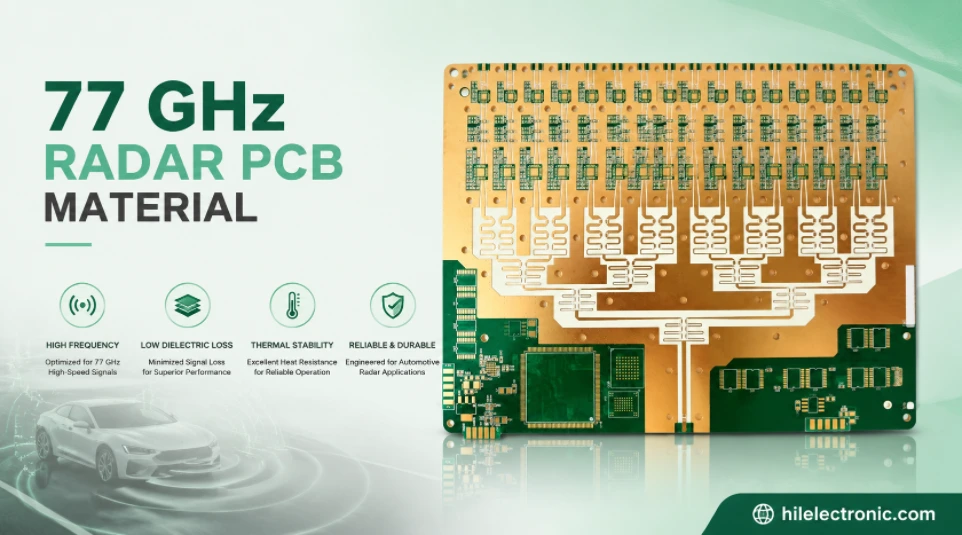
77 GHz Radar PCB Material Selection and Manufacturing Guide
Table of contentsWhat 77 GHz Changes in a PCBCommon 77 GHz...
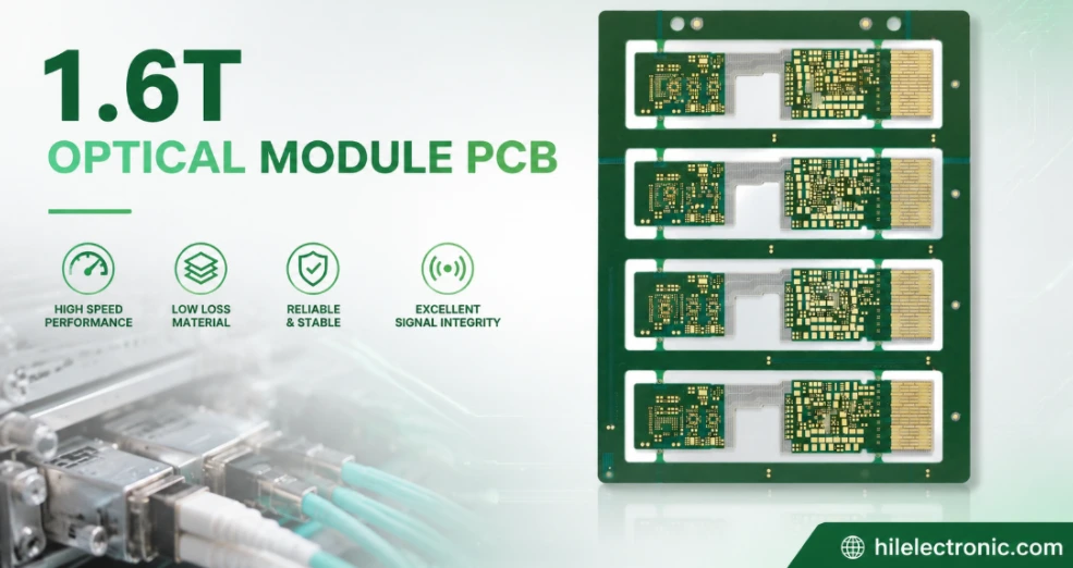
1.6T Optical Module PCB Manufacturing and Assembly Service
Table of contents1.6T Module Architectures and PCB...
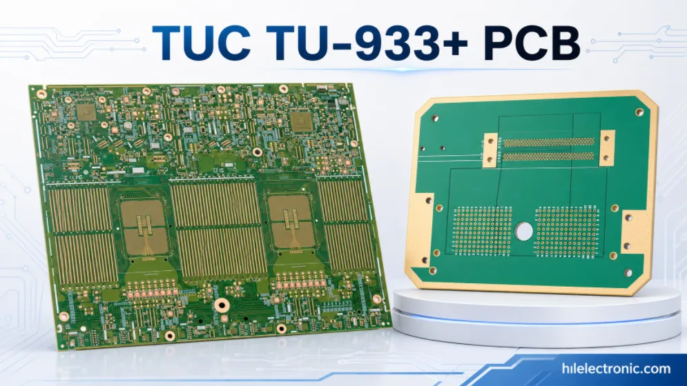
TUC TU-933+ PCB Manufacturing for Super-Low-Loss High-Speed Systems
Table of contentsWhat Is TU-933+ PCB Material?Why TU-933+...
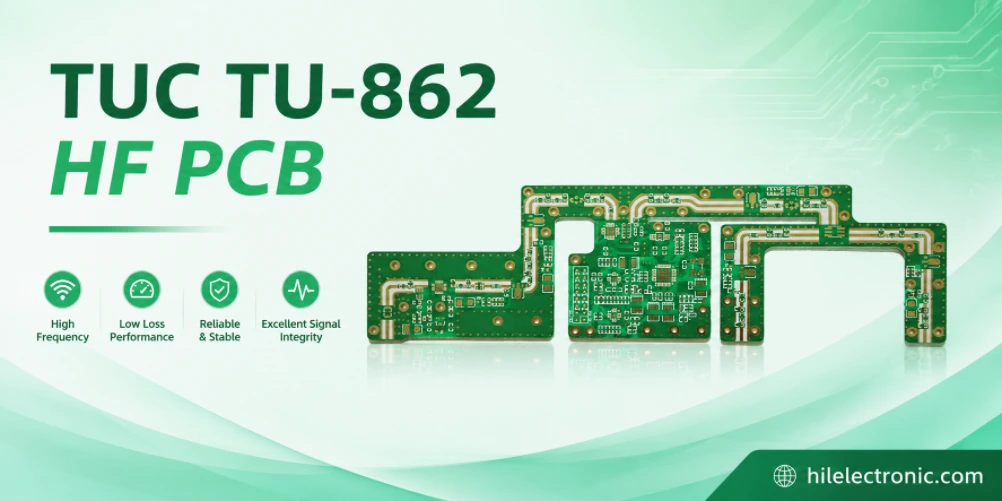
TUC TU-862 HF PCB Manufacturing and Assembly Service
Table of contentsWhat Is TU-862 HF?Why Choose TU-862 HF...
How to get a quote for PCBs
Let‘s run DFM/DFA analysis for you and get back to you with a report. You can upload your files securely through our website. We require the following information in order to give you a quote:
-
- Gerber, ODB++, or .pcb, spec.
- BOM list if you require assembly
- Quantity
- Turn time
In addition to PCB manufacturing, we offer a comprehensive range of electronic services, including PCB design, PCBA, and turnkey solutions. Whether you need help with prototyping, design verification, component sourcing, or mass production, we provide end-to-end support to ensure your project’s success.
For PCBA services, please provide your BOM (Bill of Materials) and any specific assembly instructions. We also offer DFM/DFA analysis to optimize your designs for manufacturability and assembly, ensuring a smooth production process.