
Keyboard Matrix PCB Design & Manufacturing | Anti-Ghosting
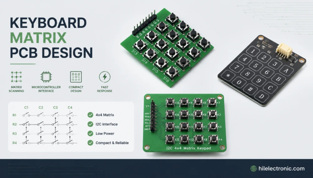
Keyboard matrix PCB design converts a large number of switches into a practical set of controller row and column signals. The matrix, diode direction, scan timing, debounce, optional layout positions and firmware pin map must describe one consistent product. A routing error may affect only one key, an entire row, a column or a specific multi-key combination, so production testing has to go beyond bare-board continuity.
Highleap Electronics supports keyboard PCB fabrication, PCBA assembly, firmware programming and matrix test-fixture development for mechanical keyboards, keypads and control panels. Customers can request an initial quotation using the key count, layout and expected quantity; a complete schematic is not required for the first contact.
Many keyboard matrices are implemented on two copper layers and may use components on both sides. A two-layer PCB is not the same as single-sided assembly, and matrix routing should not be described as requiring a single-sided board simply because switches are visible on the top.
Start a Keyboard Matrix PCB Quote
Tell us the key count or layout, approximate quantity, wired or wireless requirement and whether you need PCB fabrication, assembly, programming or testing. Attach a matrix drawing, Gerber, photo or reference only if available. No schematic is required for the initial quote.
Keyboard Matrix Architecture and Design Inputs
Rows and columns reduce pin count by scanning intersections rather than assigning one MCU pin to every key. The matrix dimensions should be selected with MCU GPIO availability, physical routing, firmware support and optional key positions in mind. An efficient matrix is not always the smallest mathematical rectangle; a slightly larger matrix can produce cleaner routing or better variant support.
| Design input | Why it matters | Release evidence |
|---|---|---|
| Row/column map | Links physical switch positions to MCU pins | The matrix mapping and firmware definition use the same row and column names. |
| Optional layouts | Can create shared electrical positions or unused intersections | Variant matrix is documented; no ambiguous duplicate key events. |
| Connector or split link | Extends rows/columns to another board or module | Pinout, protection and cable behavior are specified. |
| Test points | Allows fixture access without installing all switches | Pad size, location and net names are included in test documentation. |
Keyboard Matrix PCB Procurement and Design Inputs
The first quotation does not need a completed electrical package, but the production release eventually needs an unambiguous key-position definition. The most useful early information is the physical layout, approximate key count, required interfaces and whether the customer already has firmware. Highleap can then identify whether the project is a simple matrix build, a layout conversion or a controller-plus-firmware production package.
| Input | Why it matters | Acceptable first-inquiry form |
|---|---|---|
| Physical key layout | Defines switch centers, optional positions and likely matrix size. | Image, KLE-style layout, drawing or reference keyboard. |
| Rollover target | Affects diode population, firmware and validation combinations. | State ordinary typing, gaming/NKRO or customer-defined combinations. |
| Controller strategy | Determines available GPIO, scan rate and firmware ecosystem. | MCU name if selected, otherwise wired/wireless and firmware preference. |
| Supply scope | Separates bare PCB, assembled matrix, programmed PCBA and complete test. | Choose the closest service level. |
Diodes, Ghosting and Key Rollover
Why ghosting occurs
Without isolation, certain three-key combinations can create an unintended current path that appears as a fourth key. Matrix diodes limit current direction and are commonly fitted per switch when robust multi-key operation is required. Their orientation must match both the matrix definition and firmware scan direction.
Anti-ghosting is not identical to NKRO
Per-key diodes remove a major electrical cause of ghosting, but the final rollover behavior also depends on firmware, USB HID report format, wireless protocol and the specific combinations tested. Marketing claims should therefore be tied to an approved test plan, not inferred only from the PCB artwork.
Optional layouts create hidden matrix risk
A universal PCB may include ANSI/ISO enter, split backspace, split spacebar or alternative bottom-row positions. Mutually exclusive switch footprints can share a matrix node, but the assembly drawing and firmware must identify which positions are actually fitted. Uncontrolled optional positions can create duplicate keys, impossible combinations or a test fixture that presses the wrong coordinate.
- Specify diode orientation with a clear cathode mark and assembly drawing.
- Keep optional positions from creating unintended parallel paths.
- Verify multi-key combinations selected from the actual product use case.
- Define whether the acceptance target is 6KRO, NKRO or a customer-specific test set.
Row/Column Routing, Scanning and Firmware Correlation
Matrix signals are relatively low speed, but poor layout can still create manufacturing and EMC problems. Long parallel runs can couple LED switching noise; vias placed under switch pins may reduce mechanical clearance; traces routed too close to board edges or mounting holes can be damaged during depanelization or assembly. Highleap reviews spacing, hole relationships, diode access and test-point placement during DFM review.
- Keep the row/column naming consistent across PCB labels, firmware and fixtures.
- Place diodes with a visible polarity reference and machine-readable orientation.
- Avoid routing that requires unnecessary neck-downs around repeated switch holes.
- Provide test access for row and column nets where fixture diagnosis is expected.
- Separate noisy LED power paths from sensitive controller reset, oscillator and USB regions.
Matrix traces are generally low speed, but routing still affects manufacturability, EMI susceptibility, connector congestion and test access. Many keyboard boards are two-layer PCBs, although dense RGB, wireless modules or complex control sections may require additional layers. Ground pours should not be used as an excuse to leave narrow return bottlenecks or poorly placed stitching around noisy power and USB areas.
| Routing issue | Potential result | Recommended control |
|---|---|---|
| Long parallel row/column runs near LED or clock lines | Coupled noise or difficult fault isolation | Use sensible spacing, defined return paths and grouped net naming. |
| Diodes hidden under sockets or plates | Inspection and rework difficulty | Orient consistently and preserve AOI/visual access where possible. |
| Shared footprints for many variants | Copper stubs and ambiguous assembly | Document fitted/not-fitted positions and run variant-specific tests. |
| No test access | Slow manual diagnosis | Add matrix or MCU test points compatible with a fixture. |
Scanning, Debounce and Firmware Correlation
The hardware release must match the firmware matrix definition. Row pins, column pins, diode direction, bootloader, keymap and product variant should carry revision identifiers. Debounce settings should be validated with the actual switch or contact technology rather than copied blindly from a different keyboard.
For QMK/VIA or customer firmware, Highleap can load an approved binary and verify the physical-to-logical key map. Firmware development and algorithm ownership remain customer-defined unless separately included in the project scope.
Keyboard Matrix Design Review Checklist
| Review item | Question | Why it matters |
|---|---|---|
| Matrix size | Do row/column counts match every physical and optional key? | Prevents unmapped or duplicated positions. |
| Diode direction | Do PCB markings, assembly orientation and firmware scan direction agree? | Avoids entire-board or multi-key failures. |
| GPIO use | Are boot, debug, USB and peripheral pins protected from conflicts? | Preserves programming and recovery. |
| Optional layouts | Are mutually exclusive keys clearly defined by SKU? | Keeps BOM, firmware and fixture synchronized. |
| Test points | Can row/column faults be isolated without probing fine MCU pins? | Reduces diagnosis and rework time. |
PCB Fabrication, Assembly and Test-Fixture Development
Repeated switch and diode patterns make keyboard matrices well suited to automated assembly, but repeated patterns can also hide systematic errors. A reversed diode program or wrong feeder orientation can affect the entire board. First-article verification should therefore check polarity at multiple coordinates and confirm an actual key scan before the full lot proceeds.
Bare-board electrical test verifies copper connectivity but cannot prove matrix behavior after components and firmware are added. AOI detects many polarity and solder defects, while the functional fixture verifies the system. Both are needed for meaningful control.
No PCB schematic is required for the initial quotation. The customer can begin with the layout, key count and desired functions; detailed matrix and release data are confirmed before production.
Matrix Test Fixtures and Failure Isolation
A good fixture does more than report “keyboard failed.” It identifies the probable failure group. If every key in one row fails, the fixture or software should point toward the row net, MCU pin, series component or solder joint. If a single key fails, the diagnosis should distinguish switch or hot-swap socket contact, diode orientation, open trace and firmware mapping.
| Failure pattern | Likely area | Recommended diagnosis |
|---|---|---|
| One key does not register | Switch/socket, diode, local trace or keymap. | Probe both sides of the diode and compare raw matrix event with USB output. |
| Entire row or column fails | MCU pin, connector, common trace, solder bridge or firmware pin assignment. | Continuity and signal check from fixture point to controller. |
| Wrong key code appears | Firmware map, swapped row/column or variant definition. | Compare physical coordinate, raw scan position and released binary. |
| Failure only with multiple keys | Missing/reversed diode, firmware rollover or protocol limit. | Run approved combination matrix and inspect diode population. |
A bed-of-nails or key-actuation fixture can stimulate each switch node, read the USB or serial output and compare the result with the released key map. It should distinguish open traces, reversed diodes, solder bridges, wrong MCU pins and firmware mapping errors. Pairing an electrical net test with an application-level event test reduces false diagnosis.
- Verify power, clock and MCU programming first.
- Check row and column idle states.
- Stimulate every matrix intersection.
- Run defined multi-key combinations for ghosting and rollover.
- Verify optional-layout positions only on the applicable variant.
- Record failures by net and physical key location.
NPI, Engineering Changes and Production Records
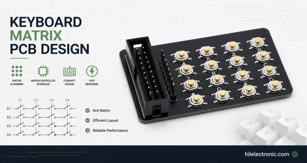
During NPI, the first assembled matrix should be verified with one controlled firmware build and a physical key-position map. Engineering changes must identify whether they alter copper, diode direction, MCU pins, bootloader, keymap or fixture software; a small PCB revision can invalidate the test program even when the outline is unchanged.
The initial quotation can start with a layout, approximate quantity and required supply scope. Before production release, the controlled package normally includes Gerber or ODB++, drill data, BOM, centroid, assembly drawings, matrix table, firmware binary, keymap and test requirements.
Stable matrix, firmware and variant definitions improve panel efficiency, component purchasing and fixture reuse. Alternate diodes, MCUs and connectors must be checked for package, polarity, electrical behavior and programming impact before release.
Matrix PCB Inspection and Test Records
When specified for the order, records can cover bare-board electrical test, diode polarity inspection, AOI, firmware revision, row/column diagnostic results, every-key output and approved rollover combinations. These records should be tied to the same PCB, firmware and product-variant revision.
Keyboard Matrix PCB Design FAQ
Why are diodes used in a keyboard matrix?
They control current direction through each switch position and help prevent unintended key paths during multi-key presses.
Do diodes automatically guarantee NKRO?
No. Diodes support anti-ghosting, but rollover also depends on firmware scanning, transport and HID report configuration.
Can a keyboard matrix PCB be two-layer?
Yes. Two-layer construction is common, although added RGB, wireless or routing constraints may justify more layers.
What should be tested in production?
Every matrix intersection, diode direction, logical key mapping, defined multi-key combinations, USB/wireless output and applicable optional positions.
Discuss a Keyboard Matrix PCB Project
Start with the key layout, approximate quantity and whether you need a bare board or complete tested PCBA. Existing drawings or files can be added later. Highleap does not require a PCB schematic for the first quotation.

Recommended Posts

Isola Astra MT77 PCB Manufacturing
Figure 1. Isola Astra MT77 PCB ManufacturingIsola Astra...

Nelco N4000-13 PCB Material and Manufacturing Guide | Highleap Electronics
Figure 1. Nelco N4000-13 PCBNelco N4000-13 PCB is a...

Copper Clad Laminate: Complete Material Selection Guide for PCB Engineers
Every electrical property that matters in a printed...

Inside a China Ceramic PCB Factory: Process Control Across Power/LED/RF/Medical
Table of Contents Inside a China Ceramic PCB Factory: How...
How to get a quote for PCBs
Let’s run DFM/DFA analysis for you and get back to you with a report. You can upload your files securely through our website. We require the following information in order to give you a quote:
-
- Gerber, ODB++, or .pcb, spec.
- BOM list if you require assembly
- Quantity
- Turn time
For PCBA services, please provide your BOM (Bill of Materials) and any specific assembly instructions. We also offer DFM/DFA analysis to optimize your designs for manufacturability and assembly, ensuring a smooth production process.