
QMK/VIA Keyboard PCB Manufacturing & Assembly
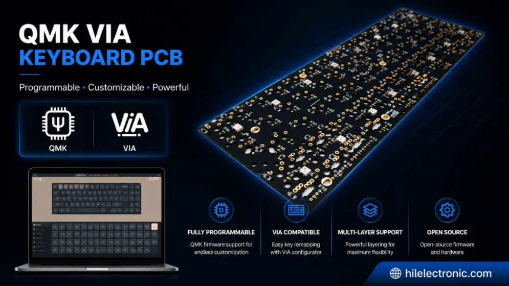
QMK and VIA are widely used in programmable keyboards, macropads and custom input devices, but reliable production depends on keeping the PCB, components, firmware and configuration files under the same revision control. Highleap Electronics manufactures bare PCBs and assembled PCBAs for a wide range of consumer, industrial, IoT, communication and control products. Within that broader capability, QMK/VIA projects can include component sourcing, SMT and THT assembly, MCU and USB-C integration, hot-swap sockets, per-key RGB, encoders, displays, firmware programming and complete functional testing from prototype through repeat production.
A QMK/VIA keyboard PCBA cannot be released from Gerber files alone. The schematic, BOM, centroid data, matrix and diode definition, MCU pin assignment, bootloader, QMK binary, VIA definition, product variant and test procedure must describe the same hardware revision. Highleap reviews these items as one manufacturing package, verifies programmability and test access, and helps prevent boards from being assembled correctly but shipped with the wrong firmware, keymap or device definition.
QMK/VIA Keyboard PCB Buying Specifications
As part of its broader PCB fabrication and PCBA services, Highleap can deliver a VIA compatible keyboard PCB, QMK PCB assembly, USB-C QMK keyboard PCB or hot-swap QMK PCB as a bare board, programmed PCBA or box-build module. A programmable keypad PCB and QMK macro keyboard PCB can use the same controlled firmware process, while each sellable variant retains its own BOM, binary and VIA definition.
| Procurement item | Highleap supply and quotation basis |
|---|---|
| Hardware scope | Matrix keyboard, programmable keypad, macropad, encoder/display controller or customer-defined QMK product. |
| Firmware package | Bootloader, released QMK binary, pin/matrix definition, VIA definition and recovery procedure. |
| PCB/assembly options | USB-C, hot-swap sockets, soldered switches, per-key RGB, encoders, displays and daughterboards. |
| Production test | Programming, enumeration, every key, diode direction, layers/modes, RGB, encoder/display and VIA recognition. |
| Supply models | Bare PCB, consigned assembly, partial turnkey, full turnkey PCBA or finished product integration. |
| Prototype MOQ | Small QMK/VIA builds can enter Highleap’s low-volume program from 5 PCBAs. MCU availability, hot-swap socket trays, RGB reels, variant count and programming fixtures determine whether a larger pilot is more cost-effective. |
| Lead-time commitment | The QMK/VIA schedule is released after PCB DFM, MCU and socket sourcing, bootloader/binary verification, VIA definition and functional-test readiness. Highleap’s lead-time guide explains the manufacturing phases; firmware changes after release trigger a revised plan. |
| Cost drivers | Key count, hot-swap sockets, RGB quantity, MCU availability, displays/encoders, variant count, programming and fixture time. |
| Preferred quotation files | Submit Gerber X2/RS-274X or ODB++, drills, BOM, centroid, drawings and schematic together with matrix/pin definitions, bootloader, production binary, VIA definition and test procedure. The Highleap file specification covers naming, units and revision consistency. |
| Firmware limitation | Highleap flashes and verifies the approved release. New QMK features, keymap development or host-software design require a separate engineering scope. |
The Highleap capability table provides the rigid-board manufacturing envelope. QMK/VIA feasibility is narrowed by matrix routing, controller package, USB-C, socket pads, RGB density, board outline and fixture access; the approved design rules are returned during DFM.
QMK/VIA Production Files, Definitions and Firmware
QMK scans the physical switch matrix and converts key events into USB HID reports. VIA adds runtime configuration based on a keyboard definition that describes the layout and configurable elements. The official VIA specification states that the keyboard definition is a JSON file containing the physical layout, layout options and elements such as encoders or lighting: VIA keyboard definition specification.
For QMK/VIA keyboard production, Highleap can combine QMK firmware flashing with matrix testing and VIA software recognition. A QMK/VIA PCBA is released only when the binary, bootloader, definition and PCB revision match; a generic “QMK compatible” note is not sufficient production control.
For compact products with encoders or displays, the same release discipline is applied in custom macropad PCB manufacturing.
| Controlled input | Production failure if missing | Highleap release check |
|---|---|---|
| Matrix map and diode direction | Wrong or ghosted key positions | Compare schematic, PCB, firmware and fixture map. |
| MCU and bootloader | Cannot program or recover units | Approve device, flash interface and image sequence. |
| USB VID/PID and descriptors | Host or VIA does not identify the product correctly | Verify approved firmware and target host. |
| VIA JSON definition | Layout options or controls appear incorrectly | Validate the production definition and version. |
| Hardware variants | Wrong image loaded to solder/hot-swap or regional layout | Use unique assembly and firmware identifiers. |
| Factory test mode | Production cannot exercise all positions efficiently | Provide fixture command or dedicated test image. |
Highleap can assemble early prototypes while the firmware evolves, but the volume release requires a frozen hardware revision, binary or reproducible source state, VIA definition and pass/fail map.
Keyboard Matrix, Diodes and Anti-Ghosting Verification
A row-column matrix reduces the number of MCU pins, but incorrect diode direction, row/column mapping or unused positions can create missing keys and ghosting. QMK’s official matrix guide explains matrix scanning and how per-switch diodes prevent unintended key combinations: QMK keyboard matrix documentation.
The finished matrix map becomes the basis of Highleap’s keyboard PCBA testing fixture.
- cross-check row and column names between schematic, PCB and QMK configuration;
- verify diode polarity, footprint rotation and assembly drawing;
- identify optional layout positions and ensure the fixture does not report them as failures;
- define direct-pin, encoder, knob, display and LED channels separately from the key matrix;
- include reset, boot and programming access that remains reachable after assembly;
- provide a test map that reports the physical key position, not only the firmware keycode.
For complex matrices, Highleap can use a bed-of-nails or mechanical key fixture. Smaller orders can use guided manual actuation with software logging, depending on test time and risk.
MCU, USB-C and Programmable Keyboard PCB Review
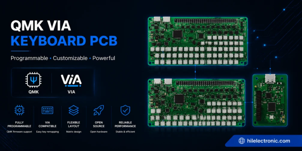
QMK/VIA products may use AVR, ARM, RP2040 or other supported controllers. Highleap reviews the exact package, crystal, decoupling, boot circuitry and programming interface. USB-C designs also require correct receptacle footprint, CC configuration, ESD protection, mechanical support and differential routing.
| Circuit area | DFM/assembly concern | Functional check |
|---|---|---|
| MCU package | Fine pitch, exposed pad, oscillator and programming access | Flash, verify and recover bootloader. |
| USB-C connector | Shell joints, alignment and case loading | Power, enumeration and cable orientation. |
| ESD protection | Correct orientation and low-capacitance data path | USB function and visual inspection. |
| Power regulation | LED and peripheral load margin | Voltage and current under defined modes. |
| External memory | Firmware or configuration storage | Read/write and retention test if used. |
| Reset/boot controls | Access after final assembly | Enter boot mode and reflash sample units. |
Relevant connector requirements can be reviewed with USB-C connector guidance and the assembly process with IC programming services.
QMK/VIA Keyboard PCB Manufacturing Specifications
The following values are taken from the published Highleap rigid PCB capability table. They are factory-level limits, not a promise that every extreme can be combined in one build. For QMK/VIA products, practical limits are driven by switch pitch, hot-swap sockets, MCU density, USB-C, stabilizer holes, long-board flatness and panel support.
Choc and other slim switch products use the mechanical controls in low-profile keyboard PCB manufacturing, while socketed builds are reviewed against hot-swap PCB requirements.
| Manufacturing item | Published Highleap capability | Project condition |
|---|---|---|
| Maximum layer count | Up to 60 layers | Actual stackup is released after DFM review. |
| Minimum inner/outer trace and space | 2/2 mil | Copper weight, board size and process combination can change the practical limit. |
| Finished board thickness | 0.2–8.0 mm | Keyboard mechanical stack and connector height usually control the selected thickness. |
| Finished board size | 10 × 10 mm minimum; 22.5 × 47.5 in maximum | Panel utilisation, outline shape and assembly support must be reviewed. |
| Outline tolerance | ±0.1 mm | Critical switch, plate and enclosure interfaces should be dimensioned on the drawing. |
| Minimum mechanical drill / annular ring | 0.15 / 0.127 mm | Use practical holes and annular rings for switch, stabilizer and connector reliability. |
| Minimum SMT pad capability | 7 × 10 mil | Component package and paste aperture remain subject to assembly review. |
| Minimum BGA pitch | 7 mil | Final package assembly depends on pad design, stencil, via strategy and inspection plan. |
| Published surface finishes | ENIG, ENEPIG, OSP, HASL, immersion silver/tin, hard gold and others | Finish is selected for solderability, contacts, cost and storage requirements. |
| Bow and twist | 0.3% | Thin or long keyboard boards require panel and fixture review to maintain flatness. |
Highleap can manufacture soldered-switch and hot-swap versions as separate controlled assemblies. Surface finish, solder mask and pad design are selected around the actual switch or socket process, not a generic keyboard assumption.
Firmware Programming, VIA Recognition and Key Testing
The factory test starts with a known firmware state. Highleap can flash the bootloader and application, verify USB identification, load or validate the VIA definition, and test all physical inputs. The program can include functional testing and stored results.
- Blank-device programming: load bootloader and application image.
- USB enumeration: confirm VID/PID, descriptors and reconnect behavior.
- VIA connection: verify that the approved definition exposes the correct layout and controls.
- Matrix test: actuate every required position and check stuck/open channels.
- Peripheral test: encoders, displays, RGB, underglow, indicators and media controls.
- Recovery test: enter bootloader or reset mode on sample units.
- Traceability: record hardware, firmware and VIA definition revision.
A dedicated factory image may speed testing, but the customer should approve whether units ship with that image or receive the release firmware after test.
Representative QMK/VIA Product Configurations
These configurations illustrate how QMK/VIA production control changes with product complexity.
| Representative configuration | Typical hardware scope | Production and acceptance focus |
|---|---|---|
| Wired programmable board | USB-C, matrix diodes, MCU and customer QMK firmware | Bootloader, enumeration, full-key test and recovery access. |
| Hot-swap RGB product | Hot-swap sockets, per-key RGB and VIA support | Socket solder inspection, LED sequence, key actuation and VIA recognition. |
| QMK macro controller | Keys, encoders, OLED/display and programmable layers | Mixed assembly, encoder/display test, firmware loading and configuration validation. |
MOQ, Cost, Lead Time and Variant Control
Keyboard products often share one PCB platform across soldered, hot-swap, ANSI/ISO or regional variants. Highleap prevents cross-loading by assigning separate BOM, assembly and firmware identifiers. A common PCB is acceptable only when all unpopulated and optional positions are clearly controlled.
Engineering builds can move through PCBA prototyping before the firmware and variant package is released for volume.
| Variant risk | Control method | Evidence |
|---|---|---|
| Wrong layout firmware | Variant-specific binary and barcode | USB/VIA verification result. |
| Wrong hot-swap or solder BOM | Separate assembly part number | AOI and first-article record. |
| Wrong LED orientation or count | Controlled centroid and firmware option | Lighting test. |
| Changed MCU or memory | Approved alternate and new firmware build | Programming and regression test. |
| Updated VIA definition | Versioned JSON and release note | Recognition and layout check. |
| Customer field update | Documented boot/recovery method | After-sales instruction and retained image. |
Prototype, NPI and repeat production are quoted with separate milestones where appropriate. Highleap maintains the approved data package so a later order does not rely on undocumented operator knowledge.
Highleap Links Hardware and Firmware Production Data
- Gerber, BOM, matrix definition, bootloader, binary and VIA files are checked for revision consistency.
- Programming and functional test are performed after assembly rather than left to the buyer.
- Hot-swap sockets, RGB, encoders and displays receive feature-specific inspection.
- Prototype and production variants can share controlled tooling without mixing firmware or labels.
- Turnkey PCBA and box-build options reduce handoffs between PCB, assembly and firmware suppliers.
QMK/VIA Keyboard PCB Manufacturing FAQ
The following questions cover the technical and purchasing issues commonly searched before moving a QMK or VIA keyboard PCB from prototype files into repeatable PCBA production.
What is the difference between a QMK keyboard PCB and a VIA-compatible keyboard PCB?
QMK is the firmware platform that controls the keyboard, while VIA provides a user-facing configuration interface for supported QMK devices. A PCB may run QMK without appearing in VIA. VIA compatibility normally requires the correct firmware features, USB identifiers and an approved device definition that matches the released hardware.
What files are needed to manufacture a QMK/VIA keyboard PCB assembly?
A production package normally includes Gerber or ODB++, drill files, schematic, BOM with approved manufacturer part numbers, centroid data, assembly drawings, matrix and diode map, MCU pin assignment, bootloader, released firmware binary, VIA definition and a functional test procedure. Enclosure and plate files are also useful when connector, socket or switch fit must be checked.
Can one QMK keyboard PCB support ANSI, ISO and multiple layout variants?
Yes, a shared PCB can support several layouts when the switch footprints, stabilizer positions, matrix assignments and mechanical clearances are designed for those options. Each sellable variant should still have a controlled BOM option, firmware or keymap, VIA definition, label and test route so production cannot mix configurations.
How are keyboard matrix diodes and anti-ghosting functions tested during production?
Manufacturing tests can verify diode orientation, row and column continuity, every switch position and the expected key event for the released matrix. Anti-ghosting behavior is primarily determined by the circuit and firmware, so the production method should define representative multi-key combinations or a customer-approved automated test script.
Can a QMK/VIA PCB include hot-swap sockets, per-key RGB, encoders and displays?
Yes. These features can be assembled on the same PCBA when the footprints, polarity, mechanical stack, power budget and firmware support are defined. High-density socket and LED arrays also need suitable stencil design, placement control and feature-specific inspection to reduce open joints, rotation and solder bridging.
How are QMK firmware versions controlled in mass production?
Each released binary should have a unique version identifier linked to the PCB revision, BOM variant and programming record. Production should verify the programmed image by checksum, readback or functional behavior, and obsolete binaries should be removed from the active work instruction to prevent mixed firmware within one lot.
How is VIA recognition verified before QMK keyboard PCBAs are shipped?
A production test can confirm USB enumeration, vendor and product identifiers, key operation and recognition by the approved VIA definition on a controlled host. Public VIA repository approval, end-user software support and future firmware maintenance remain separate from factory verification unless they are specifically included in the engineering scope.
What affects QMK keyboard PCBA prototype cost and lead time?
The main factors are PCB specification, MCU and hot-swap socket availability, RGB quantity, displays or encoders, firmware readiness, number of variants, programming access and the complexity of the full-key test fixture. Incomplete BOM data or unapproved firmware usually causes more delay than PCB fabrication itself.
Can a DIY or open-source QMK keyboard design be converted into an OEM product?
It can, provided the customer confirms design rights and supplies a production-ready, revision-controlled package. Highleap can review DFM, source components, manufacture the PCB, assemble and program the PCBA, develop production testing and support enclosure integration or box build when the mechanical and branding files are complete.

Recommended Posts

TMM4 Filter PCB Manufacturing
TMM4 filter PCB manufacturing is controlled by the...

TMM3 PCB Manufacturing for RF Modules
TMM3 PCB manufacturing is most useful where the RF module...

TMM6 PCB Fabrication
TMM6 fabrication is the process-control page for a mid-Dk...

TMM10 PCB Manufacturing for Compact RF Designs
Table of contentsHow TMM10 Shrinks RF StructuresTMM10 vs...
How to get a quote for PCBs
Let’s run DFM/DFA analysis for you and get back to you with a report. You can upload your files securely through our website. We require the following information in order to give you a quote:
-
- Gerber, ODB++, or .pcb, spec.
- BOM list if you require assembly
- Quantity
- Turn time
For PCBA services, please provide your BOM (Bill of Materials) and any specific assembly instructions. We also offer DFM/DFA analysis to optimize your designs for manufacturability and assembly, ensuring a smooth production process.