
Low-Profile Keyboard PCB Manufacturing & Assembly
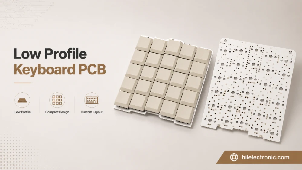
Low-profile keyboard electronics must fit a much tighter mechanical stack than standard desktop keyboards, making PCB thickness, component height and switch compatibility critical manufacturing inputs. Highleap Electronics produces bare PCBs and assembled PCBAs for many categories of electronic products. For Choc and other slim keyboard projects, services can include rigid PCB fabrication, hot-swap or soldered switch assembly, per-key RGB, USB-C, wireless and charging circuits, firmware programming, full-key testing and enclosure integration.
The switch generation, socket, keycap, plate, stabilizer, PCB outline, board thickness, connector height, battery and enclosure cannot be reviewed independently. Choc V1, Choc V2 and third-party low-profile systems may differ mechanically even when their names appear similar. Highleap verifies the approved component ecosystem and final stack before production so the finished PCBA is both electrically functional and mechanically usable.
Low Profile and Choc Keyboard PCBA Specifications
Highleap can quote a Kailh Choc PCB, low profile keyboard PCBA, thin keyboard PCB assembly or low-profile split keyboard PCB. Choc V1, Choc V2 and third-party low-profile systems are not treated as interchangeable; the approved switch, socket, plate and keycap relationship must be identified in the released drawing and BOM.
| Procurement item | Highleap supply and quotation basis |
|---|---|
| Switch system | Customer-approved Choc or other low-profile switch generation, socket or soldered footprint and matching plate/keycap. |
| PCB mechanics | Customer-specified thickness within DFM-approved capability, controlled outline, cutouts, mounting and flatness requirements. |
| Feature options | Hot-swap sockets, per-key RGB, USB-C, controller modules, wireless/BLE, batteries, encoders or displays. |
| Assembly | Repeated socket/LED arrays, mechanically loaded connectors and optional secondary assembly. |
| Test | Full-key actuation, socket presence, RGB, USB, firmware, wireless pairing and enclosure/plate fit checks as specified. |
| Prototype MOQ | Choc and other low-profile PCBAs can use Highleap’s low-MOQ program from 5 pieces. Socket packaging, switch samples, custom plates, thin-board panel support and enclosure fit fixtures can justify a different starting quantity. |
| Lead-time commitment | The low-profile schedule is set after switch/socket availability, target PCB thickness, plate/enclosure approval, RGB or wireless parts and fit-test requirements are confirmed. The assembly lead-time guide is a planning reference, not a substitute for the project commitment. |
| Cost drivers | Switch/socket ecosystem, board thickness, panel support, RGB count, wireless parts, connector reinforcement, fixture and enclosure fit inspection. |
| Preferred quotation files | Provide Gerber/ODB++, Excellon drills, BOM, centroid and assembly drawings, plus exact switch/socket data, plate and enclosure files, target thickness, firmware and fit-test criteria. Base format and revision requirements are listed in Highleap’s PCBA file guide. |
| Compatibility limitation | A similar-looking low-profile switch or socket is not substituted without customer approval and mechanical/electrical verification. |
The published Highleap rigid-board range includes thin and multilayer constructions, but low-profile products are released around board flatness, socket support, component height, plate spacing and case tolerance. The usable thickness and panel method are confirmed by DFM.
Choc and Low-Profile Switch Compatibility
Kailh Choc V1, Choc V2 and other low-profile families can differ in footprint, pins, stem, plate and keycap compatibility. The official Kailh Choc V2 page identifies a dedicated low-profile structure and SMD LED support, illustrating why the exact part number—not only “Choc”—must be controlled: Kailh Choc V2 product information.
For OEM low profile keyboard production, Highleap can supply bare boards, low profile keyboard PCBA or a tested assembly ready for case integration. A Choc keyboard PCB is released to the exact switch and socket data rather than a generic “low profile compatible” note.
Firmware and matrix variants can be controlled through the QMK/VIA keyboard PCB manufacturing process.
| Item to confirm | Why it changes the PCB or assembly | Required evidence |
|---|---|---|
| Switch generation and part number | Pin pattern, center post, LED opening and plate fit can differ | Manufacturer drawing and physical sample. |
| Soldered or hot-swap mounting | Changes pads, socket orientation and mechanical retention | Socket manufacturer drawing and switch compatibility. |
| Plate-mounted or PCB-supported design | Changes board load and installed switch stability | Plate and case stack drawing. |
| Keycap/stabilizer system | Controls spacing, cutouts and mechanical clearances | Layout and stabilizer specification. |
| LED package and direction | Low profile limits component height and light path | Approved LED and optical requirement. |
| Overall product height | Controls USB, battery, MCU and connector choices | Enclosure section and maximum component envelope. |
Highleap will not convert between Choc generations or socket systems without customer approval. A design can be electrically similar yet mechanically unusable.
Slim Board Thickness, Flatness and Mechanical Stack
Slim products create tighter relationships between PCB thickness, switch seating, plate height, keycap clearance and connector position. A thinner board can improve product height but may increase flex and assembly handling risk. Highleap reviews the complete cross-section rather than selecting thickness from the factory minimum alone.
Socketed versions are also reviewed against Highleap’s hot-swap PCB assembly requirements.
- dimension switch centers, stabilizers, mounting holes and outline from controlled datums;
- identify areas supported by the plate, tray or enclosure;
- confirm whether sockets or switch clips require a particular board thickness;
- check component height under the PCB and around batteries or foam;
- review USB-C shell height and case opening alignment;
- plan panel rails and fixtures to protect thin or long boards during reflow.
Critical outlines and holes should be marked on the drawing. Highleap can provide first-article measurements for the features that govern plate and case fit.
Low Profile Keyboard PCB Manufacturing Specifications
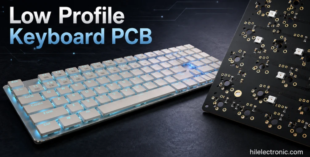
The following values are taken from the published Highleap rigid PCB capability table. They are factory-level limits, not a promise that every extreme can be combined in one build. The published minimum thickness is a factory boundary; the selected low-profile keyboard thickness must remain compatible with switch/socket mechanics, board stiffness and assembly support.
| Manufacturing item | Published Highleap capability | Project condition |
|---|---|---|
| Maximum layer count | Up to 60 layers | Actual stackup is released after DFM review. |
| Minimum inner/outer trace and space | 2/2 mil | Copper weight, board size and process combination can change the practical limit. |
| Finished board thickness | 0.2–8.0 mm | Keyboard mechanical stack and connector height usually control the selected thickness. |
| Finished board size | 10 × 10 mm minimum; 22.5 × 47.5 in maximum | Panel utilisation, outline shape and assembly support must be reviewed. |
| Outline tolerance | ±0.1 mm | Critical switch, plate and enclosure interfaces should be dimensioned on the drawing. |
| Minimum mechanical drill / annular ring | 0.15 / 0.127 mm | Use practical holes and annular rings for switch, stabilizer and connector reliability. |
| Minimum SMT pad capability | 7 × 10 mil | Component package and paste aperture remain subject to assembly review. |
| Published surface finishes | ENIG, ENEPIG, OSP, HASL, immersion silver/tin, hard gold and others | Finish is selected for solderability, contacts, cost and storage requirements. |
| Bow and twist | 0.3% | Thin or long keyboard boards require panel and fixture review to maintain flatness. |
For unusual thin-board or long-board combinations, Highleap may recommend a trial panel, temporary carrier, revised breakaway design or controlled flatness measurement before volume release.
Choc Hot-Swap Socket, RGB and Connector Assembly
Low-profile assemblies often place sockets, SMD LEDs, diodes and controllers close to switch cutouts. Highleap reviews stencil openings, component access, board support and inspection visibility for the exact hardware.
Switches, sockets, LEDs and low-profile connectors can be managed through component sourcing and AVL control.
| Assembly item | Process risk | Highleap control |
|---|---|---|
| Low-profile hot-swap socket | Insufficient solder, rotation or mechanical lift | Footprint review, paste control and AOI/manual inspection. |
| SMD LED under switch | Polarity, height and optical alignment | Centroid verification and lighting test. |
| USB-C receptacle | Shell coplanarity and enclosure loading | Reflow/hand-solder plan, visual and functional test. |
| Controller module or MCU | Height conflict and hidden joints | 3D clearance review and X-ray where applicable. |
| Battery connector | Bottom-side height and strain | Polarity, clearance and pull/fit sample review. |
| Stabilizers and mounting hardware | Hole tolerance and solder/contact interference | Mechanical sample assembly and dimensional check. |
Highleap can support SMT PCB assembly and mixed SMT/THT. Final switch installation and plate assembly can be added when the process and supplied parts are defined.
Low Profile Keyboard PCBA Fit, Firmware and Full-Key Test
Electrical continuity does not prove that a low-profile board fits its plate and case. Highleap recommends an approved mechanical first article using the production switch, socket, stabilizer and enclosure components.
The fit and electrical checks can be combined in a dedicated keyboard PCBA testing plan.
- Bare-board check: electrical test, outline and critical hole measurements.
- Assembly inspection: sockets, LEDs, diodes, USB and controller components.
- Firmware load: flash the approved QMK, ZMK or customer image.
- Matrix test: actuate every position and optional layout as specified.
- Lighting test: verify LED orientation, color and current mode.
- Mechanical fit: install sample switches, plate and case and inspect seating.
- Connector test: confirm USB cable insertion and enclosure alignment.
- Golden-unit approval: retain the approved mechanical and functional reference.
Highleap can link the matrix and peripheral test to existing keyboard PCB production experience without targeting that broad keyword on this page.
Representative Low-Profile Product Configurations
These configurations show how the mechanical stack changes the manufacturing route.
| Representative configuration | Typical hardware scope | Production and acceptance focus |
|---|---|---|
| Wired Choc hot-swap board | Low-profile sockets, USB-C and optional per-key RGB | Socket paste/support, board flatness, full-key test and case fit. |
| Wireless slim keyboard PCBA | BLE SoC/module, battery, charging and low-profile switches | Antenna keepout, component height, current, pairing and mechanical stack. |
| Low-profile split pair | Choc-compatible left/right PCBAs with displays or encoders | Pair identity, socket fit, interconnect/pairing and enclosure alignment. |
MOQ, Prototype Lead Time, Cost and Change Control
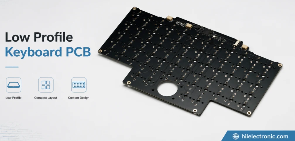
Low-profile switch ecosystems change rapidly. A switch color or generation change can alter pins or mechanical behavior even when the product name appears similar. Highleap uses an approved-vendor list and revision-controlled samples to protect repeat orders.
Initial mechanical builds can be ordered through prototype PCB production before the full assembly route is released.
| Production stage | Primary decision | Buyer protection |
|---|---|---|
| Prototype | Confirm switch/socket/plate/PCB fit | Avoids volume tooling around the wrong footprint. |
| NPI | Approve stencil, board support, firmware and key fixture | Stabilises assembly yield. |
| Volume | Use controlled parts and stored inspection/test results | Protects repeatability. |
| Component change | Compare drawing, sample and mechanical stack | Prevents silent incompatibility. |
| PCB revision | Repeat fit and firmware regression where affected | Maintains product integration. |
| After-sales | Retain approved switch/socket references | Supports replacement and failure analysis. |
Lead time is committed after the exact switches, sockets, key components, firmware and mechanical sample availability are confirmed. Split delivery or customer-supplied switches can be considered when they improve schedule control.
Highleap Controls the Entire Low-Profile Stack
- Switch, socket, plate, keycap and PCB thickness are reviewed as one mechanical system.
- Thin-board panel support and connector reinforcement are included in DFM.
- Repeated socket and RGB arrays receive dedicated stencil and inspection planning.
- Firmware and complete key tests can be combined with enclosure fit checks.
- Prototype revisions can transition to scheduled production without changing the approved stack.
Low-Profile and Choc Keyboard PCB Manufacturing FAQ
These questions cover long-tail purchasing and design concerns for thin keyboard PCBAs, including Choc compatibility, PCB thickness, hot-swap sockets, wireless integration and enclosure fit.
What is the difference between Choc V1 and Choc V2 keyboard PCB footprints?
Choc V1 and Choc V2 switches differ in mechanical details, pin arrangements and compatible keycap or plate systems. They should not be treated as interchangeable without checking the exact manufacturer drawing, socket, stabilizer, plate opening and keycap stack.
How thin can a low-profile keyboard PCB be manufactured?
The practical thickness depends on board size, layer count, copper weight, panel support, routing density, connector loads and flatness requirements. Thin boards may flex during assembly or use, so the target thickness should be reviewed together with the plate, standoffs and enclosure rather than selected only for overall height.
Can low-profile Choc keyboard PCBs use hot-swap sockets?
Yes, when the exact socket and switch generation are defined. The footprint, paste opening, orientation, plate relationship and available component height must be checked. Production testing should confirm every socket position after reflow.
What mechanical files are needed for a slim keyboard PCBA?
In addition to Gerber, schematic, BOM and centroid files, provide the switch and socket drawings, plate, keycap and stabilizer information, PCB thickness, enclosure model, mounting points, connector openings and battery dimensions. A complete stack drawing helps identify interference before assembly.
Can a low-profile keyboard PCB include Bluetooth and a rechargeable battery?
Yes. BLE, charging, protection and battery connectors can be integrated, but antenna clearance and battery thickness may be difficult in a slim enclosure. Sleep current, charging behavior, cable routing and safe mechanical retention should be included in the design and test plan.
How is low-profile keyboard PCB flatness controlled?
Panel design, material selection, copper balance, board thickness and assembly profile all influence flatness. The acceptable limit should be tied to switch alignment, plate support and enclosure mounting. Very long thin boards may need dedicated panel support or mechanical inspection.
Can per-key RGB be assembled on a thin Choc keyboard PCB?
Yes, provided the LED package, orientation, light opening, power budget and available height are compatible with the switch and plate. High-density LED arrays need accurate stencil design, polarity control and a complete lighting test.
What affects the cost and MOQ of low-profile keyboard PCBA?
Custom thin-board construction, long PCB dimensions, Choc socket packaging, RGB count, wireless parts, batteries, plates, fit fixtures and full-key testing influence cost. A small prototype build may be possible, but custom mechanical parts can set a higher practical order quantity.
Can a low-profile keyboard PCBA be tested inside the final enclosure?
Yes. Highleap can include plate and enclosure fit, connector alignment, key actuation, RGB, USB or wireless tests when the approved case, fasteners and mechanical acceptance criteria are provided.

Recommended Posts

TMM4 Filter PCB Manufacturing
TMM4 filter PCB manufacturing is controlled by the...

TMM3 PCB Manufacturing for RF Modules
TMM3 PCB manufacturing is most useful where the RF module...

TMM6 PCB Fabrication
TMM6 fabrication is the process-control page for a mid-Dk...

TMM10 PCB Manufacturing for Compact RF Designs
Table of contentsHow TMM10 Shrinks RF StructuresTMM10 vs...
How to get a quote for PCBs
Let’s run DFM/DFA analysis for you and get back to you with a report. You can upload your files securely through our website. We require the following information in order to give you a quote:
-
- Gerber, ODB++, or .pcb, spec.
- BOM list if you require assembly
- Quantity
- Turn time
For PCBA services, please provide your BOM (Bill of Materials) and any specific assembly instructions. We also offer DFM/DFA analysis to optimize your designs for manufacturability and assembly, ensuring a smooth production process.