
USB-C Keyboard PCB Manufacturer | ESD & Power Protection
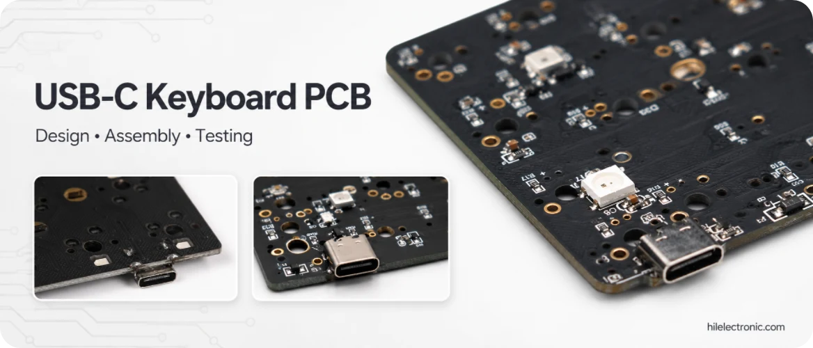
A USB-C keyboard PCB manufacturer must control the connector as an electrical interface, an ESD entry point and a mechanically stressed component. Correct USB-C operation requires more than replacing a Micro-USB footprint: CC configuration, reversible USB 2.0 data mapping, VBUS protection, shield strategy, connector land pattern and enclosure support all affect field reliability.
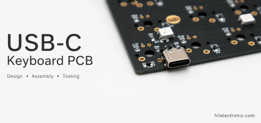
Highleap Electronics manufactures and assembles USB-C keyboard PCBAs with MCUs, ESD devices, fuses or current limiters, per-key RGB, hot-swap sockets and optional charging or wireless circuits. Production testing can cover cable orientation, enumeration, controller bootloader access, key input, current draw and connector stability.
Most standard keyboard products can be implemented on a two-layer PCB, although dense RGB, wireless or daughterboard designs may use more layers. Components can be assembled on both sides regardless of copper-layer count. Highleap can begin an initial quote from the keyboard format, connector position and quantity; no PCB schematic is required.
Start a USB-C Keyboard PCB Quote
Share the keyboard type, USB-C location, approximate quantity and whether you need PCB or PCBA. A connector reference, photo, sample or production file can be attached when available. Incomplete files are acceptable and no schematic is required for the first quotation.
USB-C Interface Requirements and Project Inputs
A typical USB 2.0 keyboard is a USB device or sink. CC1 and CC2 require the appropriate device-side configuration, commonly pull-down resistors when not integrated elsewhere in the approved design. D+ and D− from both connector orientations must be connected according to the connector pinout and routed as a controlled pair with minimal stubs. The exact implementation should follow the selected connector, MCU or USB interface reference design.
| Interface item | Production risk | Control |
|---|---|---|
| CC1/CC2 configuration | No power or unreliable orientation detection | Verify approved component values and fitted parts against the released USB-C device design. |
| D+/D− routing | Enumeration instability or emissions | Maintain pair geometry, short protection path and correct connector pin mapping. |
| Shield connection | ESD or noise path enters logic ground unpredictably | Define chassis/ground connection and enclosure relationship. |
| VBUS sensing/power path | Back-powering or overstress | Use the approved protection and power-path architecture. |
USB-C Keyboard PCB Buying Specifications
The quotation should separate a simple USB 2.0 keyboard device from products that also charge a battery, operate wirelessly, drive a large per-key RGB load or use a separate USB daughterboard. These variants may look similar at the connector but require different power paths, protection parts and tests.
| Project item | Manufacturing impact | What to provide initially |
|---|---|---|
| Connector position | Controls PCB edge, enclosure opening, cable access and mechanical load path. | Top, side, daughterboard or reference photo. |
| Operating modes | USB-only and charge-plus-wireless designs use different power architectures. | Wired, wireless or tri-mode. |
| Maximum load | Per-key RGB, displays and charging influence VBUS current and thermal margin. | Approximate feature list; exact current can follow later. |
| Connector strategy | Main-board connector and detachable daughterboard require different cables and tests. | State preferred architecture if known. |
Layout, ESD, Grounding and Power Protection
CC1 and CC2 must reflect the device role
A keyboard is normally a USB device/sink. The approved design must present the correct device-side CC behavior, whether implemented with discrete pull-down resistors or integrated circuitry. Missing or incorrect CC components can prevent power delivery or cause orientation-dependent operation.
Reversible data mapping needs both plug orientations
For USB 2.0, the duplicated D+ and D− pins on a receptacle must be connected according to the connector data sheet. Stubs should be minimized, the pair should remain coupled and the ESD device should be placed close to the connector. A board that enumerates in one cable orientation can still be assembled incorrectly.
ESD current needs a deliberate return path
Installing a TVS array is not enough if the discharge path runs through sensitive logic ground or uses long vias and traces. Shield connection, chassis relationship, ground stitching and enclosure material should be reviewed as one system. Highleap assembles the approved protection network and can perform customer-defined ESD protection validation at product level when included in the project.
ESD suppressors should be located close to the connector with a short return path. The power input may also use a fuse or current limiter, transient suppression, reverse-current blocking and regulated rails depending on the architecture. “Reverse plug protection” for USB-C is mainly achieved by the symmetrical connector and correct pin implementation; it should not be confused with reverse-polarity protection for a raw DC input.
- Select low-capacitance ESD protection suitable for USB 2.0 data lines.
- Keep the protected path short and avoid routing the surge through sensitive MCU ground.
- Define VBUS current and brightness limits for RGB-heavy products.
- Prevent external batteries or alternate supplies from back-feeding the USB port.
Connector Mechanics, Daughterboards and Enclosure Integration
USB-C connectors vary in shell tabs, pegs, overhang and hybrid SMT/PTH construction. A visually similar substitute can use a different footprint or enclosure datum. The exact supplier drawing, board-edge relationship, solder access and mechanical support should be approved together.
- Use shell stakes or through-hole tabs where the selected connector and duty require them.
- Avoid enclosure geometry that side-loads the plug.
- Check daughterboard cable bend radius and strain relief.
- Verify connector height and overhang after soldering.
- Use a golden enclosure or mechanical gauge for first-article fit.
For high-use products, the pilot may include customer-defined insertion cycles, controlled cable movement or enclosure-level fit checks. These tests depend on the selected connector and product duty; they are not guaranteed by the connector family name alone.
USB-C Daughterboards and Internal Cable Control
A separate USB-C daughterboard can decouple the connector from the main keyboard PCB and make enclosure variants easier. It also introduces an internal cable, two connectors and another opportunity for pinout or orientation error. The link may carry USB D+/D−, VBUS and ground, or use a board-to-board interface defined by the customer.
- Freeze the daughterboard connector and cable pinout.
- Prevent reversed mating through keying or clear assembly control.
- Keep USB data routing and return continuity through both boards.
- Provide strain relief so external cable force does not pull the internal connector.
- Test the complete main-board/daughterboard pair, not each board only in isolation.
Charging, PCB Assembly and Production Testing
When the USB-C port also charges a battery, the keyboard needs a defined charger, battery protection and power-path behavior. The design should specify whether the keyboard can operate while charging, how current is shared between system and battery, what happens with a deeply discharged cell and how the host is protected from back-feed.
Production testing can include charge-state indication, current at selected battery conditions, wired/wireless transition and sleep current. USB Power Delivery is not automatically required for an ordinary low-power keyboard; adding PD circuitry without a real power need increases BOM and firmware complexity.
USB-C PCB Assembly and Inspection
Assembly may combine fine-pitch SMT signal pads with large shell tabs or through-hole anchors. Paste balance and reflow profile must produce reliable signal joints without floating the connector. AOI can verify alignment and visible pads; focused visual inspection or X-ray may be added when critical joints are hidden and the risk justifies it. Connector and MCU handling should also follow ESD controls during SMT assembly.
Power, Enumeration and Cable-Orientation Tests
Keyboard PCBA production testing should power and enumerate with the released firmware. Testing both plug orientations is important because a missing CC connection, duplicated data-pin fault or solder defect can leave one orientation inoperative.
- Measure VBUS input and regulated rails.
- Connect the cable in both plug orientations.
- Verify enumeration, descriptors and key input.
- Run the approved maximum RGB or peripheral load without reset.
- Check bootloader or recovery access through the same port.
- Inspect connector movement, solder joints and enclosure fit after handling.
Where charging is included, add charge-state indication, battery current, power-path transition and back-feed checks under the defined battery conditions.
Failure Diagnosis, Rework, Cost and Production Records
| Symptom | Probable cause | Verification |
|---|---|---|
| No power in either orientation | CC error, open VBUS, damaged connector or protection component. | Check CC population, VBUS path and connector joints. |
| Works in only one orientation | Missing duplicated data connection, CC fault or connector solder issue. | Test both orientations and continuity to each receptacle pin group. |
| Enumerates then resets with RGB | VBUS drop, current limit, weak regulator or firmware peak load. | Measure input and internal rails during the approved maximum pattern. |
| Intermittent when cable moves | Cracked shell/signal joints, poor enclosure alignment or damaged connector. | Observe joints under controlled cable movement and inspect load transfer. |
| MCU damaged after handling | Inadequate ESD path, unsuitable protection or grounding. | Review protection placement and perform defined system-level ESD testing. |
Connector Rework and Repair Criteria
USB-C rework needs controlled preheat, solder removal and connector lifting to avoid pad damage. After replacement, both orientations, shell stability and data operation should be retested. Boards with torn signal pads or weakened anchors require a documented repair decision rather than cosmetic touch-up.
Customization, Cost and Supply Planning
Cost is influenced by connector construction, protection network, assembly-side count, daughterboard cable, charging circuitry, inspection method and functional test time. Stable orders can reduce unit cost through connector reel purchasing, panel efficiency and fixture amortization.
The exact connector MPN should be frozen before volume quotation because a substitute can change the footprint, shell anchoring and enclosure opening. ESD devices, MCUs, laminate and charging components should also be approved early enough for pilot validation.
For repairable products, the service strategy should specify whether the USB-C connector is serviced by replacing a daughterboard or the entire PCBA. A daughterboard can simplify field replacement; an integrated connector reduces parts and internal connections. The correct choice depends on enclosure space, cable routing, expected use and after-sales strategy.
USB-C Keyboard PCBA Test Records
When included in the order, records can cover connector incoming verification, first-article connector alignment, AOI or focused joint inspection, firmware revision, current measurement, two-orientation enumeration and every-key testing. Required mechanical or ESD validation should be defined with a standard, enclosure and acceptance criteria before quotation.
USB-C Keyboard PCB FAQ
Does a USB-C connector work in both orientations automatically?
Only when CC, D+/D− and power pins are implemented correctly and the assembly is verified in both orientations.
Where should USB ESD protection be placed?
As close to the connector as practical, with short data traces and a low-impedance return path that keeps surge current away from sensitive logic.
Should the USB-C connector use through-hole shell tabs?
That depends on the selected connector and mechanical duty. Through-hole or reinforced shell features can improve load transfer, but the exact footprint must match the part.
What should be tested after assembly?
VBUS and rail voltage, both cable orientations, enumeration, key events, bootloader access, maximum approved load and connector stability.
Discuss a USB-C Keyboard PCB Project
Provide the keyboard type, connector location, approximate quantity and required service. A photo or existing design file is optional at the inquiry stage. No PCB schematic is required for an initial quotation.

Recommended Posts

Taconic RF-35 PCB Manufacturing Service — Prototype Through Volume Production
Figure 1. Taconic RF-35 PCBTaconic RF-35 is the workhorse...

Isola Astra MT77 PCB Manufacturing
Figure 1. Isola Astra MT77 PCB ManufacturingIsola Astra...

Nelco N4000-13 PCB Material and Manufacturing Guide | Highleap Electronics
Figure 1. Nelco N4000-13 PCBNelco N4000-13 PCB is a...

Copper Clad Laminate: Complete Material Selection Guide for PCB Engineers
Every electrical property that matters in a printed...
How to get a quote for PCBs
Let’s run DFM/DFA analysis for you and get back to you with a report. You can upload your files securely through our website. We require the following information in order to give you a quote:
-
- Gerber, ODB++, or .pcb, spec.
- BOM list if you require assembly
- Quantity
- Turn time
For PCBA services, please provide your BOM (Bill of Materials) and any specific assembly instructions. We also offer DFM/DFA analysis to optimize your designs for manufacturability and assembly, ensuring a smooth production process.