
Back to blog
Recycling PCBs – challenges & opportunities
Introduction
As a crucial building block of modern electronics, printed circuit boards (PCBs) underpin technologies that drive economic growth globally. However, the environmental burden of PCB waste calls for urgent industry-wide changes to align design and manufacturing with the principles of sustainability.

This article analyzes key shifts – from renewable materials to responsible end-of-life disposal – that can bolster PCB sustainability alongside innovative technologies poised to accelerate progress. It also weighs economic considerations for green transitions and suggests a collaborative roadmap to proliferate eco-friendly electronics.
Eco-Friendly Materials in PCB Design
The use of eco-friendly materials in Printed Circuit Board (PCB) design is an emerging trend reflecting the electronics industry’s growing concern for environmental sustainability. This shift involves several key changes:
- Biodegradable PCB Substrates: Traditional PCBs often utilize non-biodegradable materials such as fiberglass, which contribute to persistent environmental waste. The move towards biodegradable materials, such as paper or cellulose, marks a significant stride towards sustainability. These substrates not only reduce long-term environmental waste but also have a natural decomposition process, which minimizes the overall environmental impact of PCBs.
- Embracing Lead-Free Solder Alternatives: Historically, electronic manufacturers have used lead in solder due to its low melting point and durability. However, the adverse health and environmental impacts of lead have prompted a shift to lead-free alternatives. This change aligns with environmental regulations and reduces health hazards, supporting sustainable electronic waste management.
- Implementing Recyclable Metals: The inclusion of recyclable metals like copper and aluminum in PCB design is becoming increasingly standard. These metals can be reclaimed and reused, reducing the demand for new resources. This approach aligns with industry standards and demonstrates a commitment to conserving natural resources.
Each of these changes represents a critical step towards making PCB manufacturing more sustainable and environmentally friendly. By adopting these practices, the electronics industry shows its increasing concern for the environment and its commitment to reducing its ecological footprint.
Modular PCB Architecture for Sustainability
The concept of modular PCB architecture is a testament to sustainability in PCB design. It showcases an innovative approach that emphasizes the creation of circuit boards with easily replaceable electronic components. This strategy not only enhances the adaptability and durability of electronic products but also aligns seamlessly with environmental objectives, promoting sustainability.
Diverse Aspects of Modular PCB Architecture:
The visual representation of modular PCB architecture can be likened to an intricate collage, providing glimpses into various facets of this design philosophy. Close-ups on components such as bias tees, cold-finger feedthroughs, and detailed views of microwave connectors, filters, and SMD inductors paint a vivid picture of the technology’s complexity and ingenuity.
Key Pillars of Modular PCB Architecture for Sustainability:
- Swappable Components: The cornerstone of modular PCBs lies in their user-friendly design, featuring parts that can be effortlessly interchanged or upgraded by end-users. This adaptability enhances the versatility of electronic products and extends their functional life.
- Extended Product Lifespan: The modular approach inherently facilitates swift and efficient component replacement. This capability plays a pivotal role in extending the operational life of electronic devices. Prolonging the lifespan of these products significantly reduces electronic waste, which is a substantial environmental benefit.
- Cost Efficiency and Savings: While the initial development of modular PCBs may entail higher costs, the long-term advantages are undeniable. Modular PCBs simplify upgrades and maintenance, ultimately leading to a reduction in warranty claims and the need for product replacements. This translates to substantial cost savings over time.
- Commitment to Environmental Responsibility: Beyond its technological advancements, modular PCB design underscores a steadfast commitment to environmental responsibility. By diminishing electronic waste and encouraging the reuse and recycling of components, this design strategy provides robust support for sustainability goals. It reflects a conscious shift in the industry towards embracing eco-friendly practices, highlighting a more environmentally responsible approach to the manufacturing and design of electronic products.
Overall, modular PCB architecture stands as a shining example of how technological innovation can harmonize with sustainability objectives. Through its emphasis on adaptability, longevity, cost-efficiency, and environmental responsibility, it embodies a transformative approach that sets the tone for a more eco-conscious electronic industry. As we continue to explore and refine modular PCB design, we move ever closer to a future where electronic products are not only cutting-edge but also deeply attuned to the needs of our planet.
Pioneering Additive Manufacturing for PCBs
In the realm of green manufacturing processes, additive manufacturing, often referred to as 3D printing, emerges as a pioneering technique in PCB (Printed Circuit Board) production. This cutting-edge method involves the meticulous layer-by-layer deposition of materials, commonly polymers or metals, to craft intricate circuitry and components. Unlike traditional subtractive manufacturing processes that entail cutting away material from a larger piece, additive manufacturing embraces a more resource-efficient approach by adding material only where it’s essential.

Precise Material Deployment
At the heart of additive manufacturing’s eco-friendly appeal lies its strategic approach to material deployment. By depositing material with pinpoint accuracy only where it is needed, waste generation is dramatically minimized. This precision stands in stark contrast to conventional manufacturing methods that often result in significant material wastage.
Optimizing Resource Utilization
The incorporation of additive manufacturing techniques into PCB production represents a quantum leap in resource optimization. This method’s ability to conserve materials by utilizing them with maximum efficiency is a testament to its eco-conscious design. Rather than discarding excess material, additive manufacturing ensures that every bit serves a purpose, aligning PCB assembly processes with sustainability goals.
A Revolution in PCB Assembly
The adoption of additive manufacturing in PCB production heralds a new era for the industry, characterized by reduced environmental impact. By embracing this innovative approach, the electronics manufacturing sector not only enhances its efficiency but also substantially reduces its carbon footprint. This evolution in PCB assembly processes reflects a broader commitment to environmentally responsible manufacturing practices, setting the stage for a greener and more sustainable future.
Overall, additive manufacturing stands as a beacon of eco-friendly progress in the realm of PCB production. Its meticulous material deployment, resource optimization, and low waste generation make it a formidable force in advancing green manufacturing processes. As this technology continues to evolve and gain prominence, it paves the way for a more sustainable electronics industry, where precision, efficiency, and environmental responsibility converge to shape a brighter and greener future.
Advancing Sustainability in PCB Design and End-of-Life Management
The rapid pace of technological advancement in the electronics industry has led to a growing concern—how to responsibly manage the end-of-life disposal of electronic components, especially printed circuit boards (PCBs). PCBs are integral to nearly all electronic devices, making their recycling and sustainable design critical to reducing electronic waste. This article delves into the importance of end-of-life PCB management and highlights innovative sustainable practices in PCB design.

End-of-Life PCB Management
- Modular PCB Design for Sustainability: The concept of modular PCB architecture is at the forefront of sustainable PCB design. This approach centers on crafting circuit boards with easily replaceable components. It empowers users to swap or upgrade parts effortlessly, enhancing product flexibility, durability, and eco-friendliness.
- Responsible Disposal: PCB recycling programs offer a responsible and regulated avenue for disposing of electronic waste, significantly reducing the risk of environmental contamination.
- Resource Recovery: Recycling PCBs recovers and repurposes valuable materials, including metals and components, thereby reducing the demand for new natural resources and conserving them for the future.
- Waste Reduction: These recycling programs divert PCBs from landfills and incineration, contributing to overall waste reduction and a smaller environmental footprint.
- Compliance with Regulations: Participation in recycling programs ensures compliance with environmental regulations, promoting sustainable electronic waste management practices and reducing legal and environmental risks.
- Environmental Responsibility: Supporting PCB recycling programs reflects a commitment to environmental responsibility and sustainability in the electronics industry, fostering a greener future.
Sustainable PCB Innovations
- Modular PCB Design: Modular PCB design is gaining traction, enabling the easy swapping of replaceable components. This approach extends product adaptability and longevity, reducing electronic waste and supporting sustainability.
- Renewable Resources in PCB Production: Integrating renewable resources like paper or cellulose into PCB production is a significant step toward sustainability. It reduces dependence on finite resources and promotes eco-friendly practices.
- Energy-Efficient PCB Fabrication: Sustainable PCB manufacturing embraces energy-efficient processes, leveraging renewable energy sources and low-power methods to significantly reduce energy consumption during production.
- PCB Lifecycle Management: Comprehensive end-of-life disposal strategies are essential for responsible PCB management. These programs ensure the recovery of valuable raw materials, minimizing waste and adhering to the principles of a circular economy.
- Compliance with Environmental Regulations: Striving for compliance with environmental regulations is paramount in sustainable PCB design, ensuring the industry’s minimal negative impact on the environment and promoting responsible electronic waste management.
- Waste Reduction in Production: Managing waste generated during PCB manufacturing is crucial. Sustainable production processes prioritize waste reduction through innovative techniques and efficient resource utilization.
- Hazardous Material Reduction: Reducing or eliminating hazardous materials in PCB manufacturing is a priority for sustainability. Safer alternatives help minimize environmental and health risks.
As the electronics industry continues to evolve, embracing sustainability in PCB design and end-of-life management becomes increasingly essential. By addressing innovative approaches and considerations, the industry can make a significant contribution to a greener and more responsible future. It is a collective responsibility to ensure that our electronic devices not only enrich our lives but also preserve the environment for generations to come.
Navigating Challenges for Sustainable PCB Design
In the pursuit of sustainability in PCB (Printed Circuit Board) design, there are challenges to overcome. While incorporating sustainable materials and methods may initially involve higher costs, the long-term environmental and economic benefits are substantial. This article explores key considerations in cost implications and environmental advantages associated with sustainable PCB design. Additionally, it highlights the importance of technological advancements and ongoing research to address these challenges and uphold sustainability as a core principle in PCB design.
Cost Implications and Environmental Benefits
- Initial Costs: The adoption of sustainable materials and methods in PCB design may incur higher upfront expenses compared to conventional approaches. It is essential to acknowledge and plan for these initial costs as part of a broader sustainability strategy.
- Reduced Waste Management Costs: Sustainable practices result in reduced waste generation over time. This translates into decreased waste management expenses, as less waste needs to be disposed of, contributing to cost savings in the long run.
- High-Quality Solutions: Sustainable approaches prioritize maintaining high-quality standards. Despite the initial cost investments, sustainable PCBs continue to meet performance expectations and reliability requirements.
- Cost-Effectiveness: The crux of sustainable PCB design lies in its long-term cost-effectiveness. While the upfront investment may be higher, the overall cost savings, including reduced waste, enhanced energy efficiency, and extended product lifecycles, far outweigh this initial expenditure.
Technological Advancements and Sustainable Solutions
- Ongoing Research: Sustainable PCB design demands continuous research and development efforts. Researchers and industry experts must collaborate to identify innovative solutions and overcome challenges in materials, processes, and waste reduction.
- Advancements in Fabrication: Continuous improvements in fabrication processes are pivotal to sustainability. Technological advancements enable the development of more efficient and eco-friendly manufacturing methods, which can significantly reduce the environmental footprint of PCB production.
- PCB Layout Innovation: Innovative PCB layout designs play a critical role in sustainability. Efficient layouts maximize component utilization, minimize material waste, and optimize overall performance, aligning with sustainability objectives.
Sustainable PCB design necessitates a careful balance between initial costs and long-term environmental and economic benefits. Technological advancements, ongoing research, and innovative solutions are central to overcoming the challenges associated with sustainability in PCB design. By navigating these hurdles and embracing sustainable practices, the PCB design industry can make significant contributions to a greener and more responsible future, aligning with the broader sustainability goals of our society.
Conclusion
Furthermore, while initial costs for sustainable materials and methods may present challenges, the long-term benefits, including reduced waste management expenses and continued high-quality standards, make sustainability a cost-effective choice in the PCB design process. It is a strategic investment that not only benefits the environment but also contributes to the economic well-being of the industry.
To continue advancing towards sustainability in PCB design, ongoing research and development efforts are essential. These efforts should address emerging challenges, seek innovative solutions, and drive technological advancements in fabrication processes and PCB layout. By doing so, the electronics industry can remain at the forefront of both technological innovation and environmental responsibility, ultimately paving the way for a more sustainable and resilient future.

Related Articles
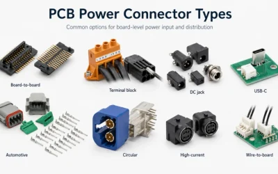
PCB Power Connector Selection: Types and Mounting
Choose PCB power connectors and board sockets with the right current rating, pitch, mounting style, and retention for reliable assembly.

Inductor Impedance: Formula, Calculation, PCB Design
Learn how to calculate inductor impedance, interpret reactance and real-world losses, and apply the result to PCB filter and power design.
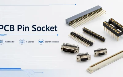
PCB Pin Socket Guide: Headers, Receptacles, IC Sockets
Choose the right PCB pin socket by comparing headers, receptacles, and IC sockets by pitch, current rating, plating, and assembly method.