
USB Modem PCB Manufacturing & PCBA for LTE/5G Dongles and Data Adapters
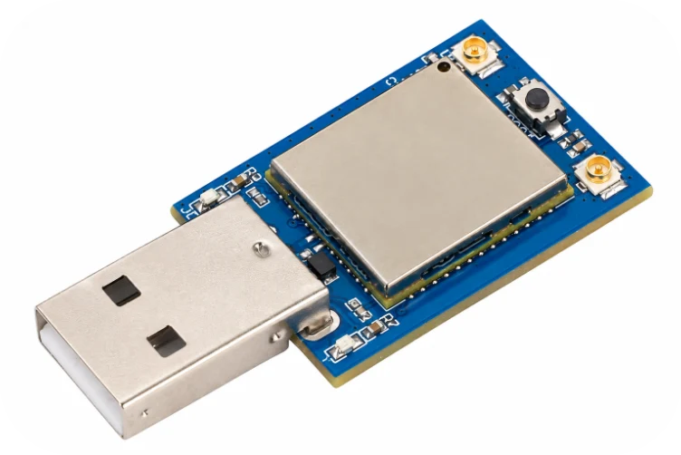
USB Modem PCB fabrication and assembly involves a compact board with two distinct interfaces: the USB connection to the host and the cellular circuitry used for LTE or 5G communication. The production package may include a direct-insert USB connector, a cellular module, SIM hardware, RF components, power conversion and an antenna connection. The actual population and board technology are defined by the product design.
Highleap Electronics provides PCB manufacturing, electronic component sourcing and PCBA assembly for OEM products in communications, industrial, consumer and other sectors. For USB modem boards, fabrication and assembly are carried out to the approved stack-up, bill of materials, drawings and project-specific acceptance requirements. Bare boards, fully populated PCBAs and coordinated sourcing-and-assembly orders can be quoted according to the required delivery scope.
USB Connector and Board-Edge Manufacturing
The connector is one of the defining parts of a USB modem board. Some dongles use a USB-A plug or an approved board-edge contact structure; others use a USB-C receptacle or a short cable connection. Each implementation has different dimensional, soldering and retention requirements.
Connector fit is controlled in the PCB and assembly drawings
For a direct-plug design, the specified board thickness, contact finish, plug position, shell attachment and enclosure clearance must agree with the mating interface. For a soldered receptacle, the approved footprint, locating features, anchor joints and seating height determine how the connector is assembled and inspected. Designs using Type-C connections should specify their actual data and power implementation; the connector alone does not establish USB speed or Power Delivery support. See the USB-C connector mounting and PCB requirements for related manufacturing considerations.
First-piece inspection can include connector alignment, mechanical seating and the permitted board-edge geometry. Electrical continuity and USB detection remain separate checks. Where the enclosure transfers insertion forces into the board, the mechanical support method belongs in the released documentation.
LTE/5G Module and RF Component Assembly
A USB cellular modem PCBA can contain a preassembled modem module or a more integrated chipset and RF front end. The SMT process, approved component list and inspection route follow the actual package specifications. SIM sockets, coaxial RF connectors, shields, oscillators and power-management parts may require secondary assembly steps or particular handling instructions.
Material control applies to RF parts as well as the modem module
RF filters, matching components, duplexers and antenna switches should be purchased against the approved manufacturer part numbers or specifically authorized alternatives. Components with the same nominal resistance or inductance are not necessarily interchangeable at the relevant radio frequencies. A substitute modem module can also change firmware, pinout, power or band-support requirements.
For high-value or customer-consigned modules, incoming quantities, part revisions, storage requirements and rework rules can be included in the manufacturing agreement. The assembly route should also identify whether a shield or RF connector is installed during reflow or in a subsequent operation. These are controlled production instructions, not changes made at the assembly line without approval.
Power, Impedance and Thermal Requirements on the PCB
Bus-powered modem electronics combine the USB supply with a cellular load that can vary during radio activity. Copper dimensions, decoupling, power components and ground structures must reproduce the released electrical design. If an approved test procedure includes an active-transmit state, the fixture supply conditions must be specified so that measurements are relevant to the product.
The USB data path and cellular RF feed can require different trace widths, references and impedance targets. Fabrication is therefore based on the customer’s net-specific impedance requirements and stack-up—not a single generic “high-frequency PCB” setting. Solder-mask openings, ground connections, RF connector launches and ESD-device placement should remain consistent with the release package. Where applicable, RF-sensitive PCB assembly controls can help identify components and soldering features needing extra attention.
A compact LTE or 5G dongle may use copper spreading, thermal vias or shielding as part of its heat path. Their geometry can be inspected at board and assembly level; continuous modem operation and enclosure temperatures are evaluated under the product’s defined validation conditions. No specific layer count, HDI structure or specialty laminate is implied solely by the cellular standard.
Highleap Electronics • PCB Manufacturing & Assembly
Bring Your PCB Design to Production with Highleap
From bare PCB fabrication to component sourcing and finished PCB assembly, get a quotation based on your files and quantities. Contact us about international delivery, after-sales assistance and practical payment arrangements for your order.
Worldwide Shipping Options
After-Sales Assistance
Payment Options by Agreement
| Get a PCB Quote | Contact Our Team |
Shipping arrangements, after-sales coverage and payment terms are confirmed for each order.
Controlled Production of Regional Modem Variants
An OEM USB modem platform may use one fabricated PCB for several regional assemblies. Approved variants can differ in the modem module, RF filter population, SIM or eSIM components, antenna connections or software image. The relevant differences belong in controlled BOMs and assembly documentation for each product SKU.
Where components are intentionally omitted, the assembly files should mark the do-not-populate positions and identify the appropriate inspection criteria. This helps keep regional builds distinct even when they share a board outline and a significant portion of the BOM. Firmware loading, device labeling and any serialization requirements are included only when specified in the order.
The same revision discipline applies to future builds: changes in PCB fabrication data, alternate components or module firmware are recorded and approved before production. An agreed PCBA first-article inspection procedure can establish the accepted physical assembly for each released configuration.
USB and Cellular Checks at PCBA Level
USB interface checks and cellular function checks verify different portions of a modem assembly. A device may enumerate at the host while its SIM interface, radio configuration or antenna path still requires verification. The factory test plan should name the functions to be checked, the required fixtures and the pass/fail limits.
- USB interface: connector continuity as specified, device identification, enumeration and required host communication.
- Modem electronics: power-up, module identity, SIM interface and firmware or configuration verification where applicable.
- Cellular functions: a defined radio or network/simulator screen only when approved equipment, authorization and acceptance criteria are available.
- Recorded results: applicable PCB revision, populated variant, programming image and agreed electrical or functional test data.
Customer-defined PCBA functional test procedures can be incorporated into an assembly quotation. Final device RF performance, operator approvals and regulatory compliance remain separate from routine board-level inspection unless a distinct scope is established.
PCB Manufacturing, Assembly and Order Delivery with Highleap
Highleap’s electronics manufacturing services cover bare-board production and assembled circuit boards across different electronic applications. USB cellular modem boards are manufactured within that wider PCB/PCBA service range, with the selected board materials, approved components and inspection requirements defined by each project.
For projects needing unified material purchasing and board assembly, turnkey PCB and PCBA production offers a coordinated supply route. Customer-supplied modules, special assembly stages, programming and test fixtures can be listed separately where required. Orders progressing to repeat quantities can use high-volume circuit board assembly planning to align material availability, controlled revisions and inspection capacity.
Manufacturing information for quotation
Submit the released Gerber or ODB++ data, stack-up and fabrication notes, approved BOM, placement files, assembly drawings and quantities per variant. For USB modem PCBAs, also include the connector specification, module part number, relevant RF or impedance notes, programming requirements and requested test method. Highleap can review the files and quote the bare PCB, sourcing and PCBA operations included in the requested manufacturing scope.

Recommended Posts
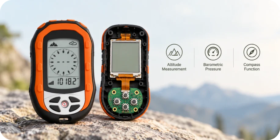
Handheld Altimeter PCB Manufacturing & Assembly for Barometric Instruments
A Handheld Altimeter PCB typically uses an absolute...
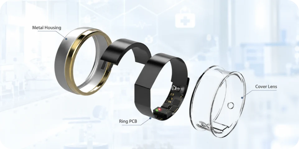
Smart Ring PCB | Compact Flex Circuit for Wearables
A smart ring PCB has to fit sensing, BLE, power and...
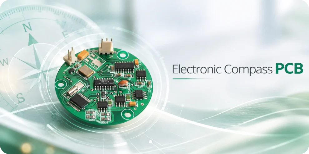
Electronic Compass PCB Manufacturing & PCBA for Digital Heading Products
An Electronic Compass PCB converts magnetometer data—and...
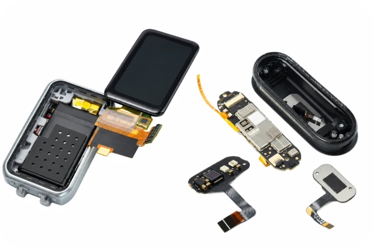
Smart Bracelet PCB Manufacturing and Assembly
A smart bracelet PCB can support very different products:...
How to get a quote for PCBs
Let’s run DFM/DFA analysis for you and get back to you with a report. You can upload your files securely through our website. We require the following information in order to give you a quote:
-
- Gerber, ODB++, or .pcb, spec.
- BOM list if you require assembly
- Quantity
- Turn time
For PCBA services, please provide your BOM (Bill of Materials) and any specific assembly instructions. We also offer DFM/DFA analysis to optimize your designs for manufacturability and assembly, ensuring a smooth production process.