
Mobile Wi-Fi Router PCB Manufacturing & Assembly for 4G/5G Hotspot OEMs
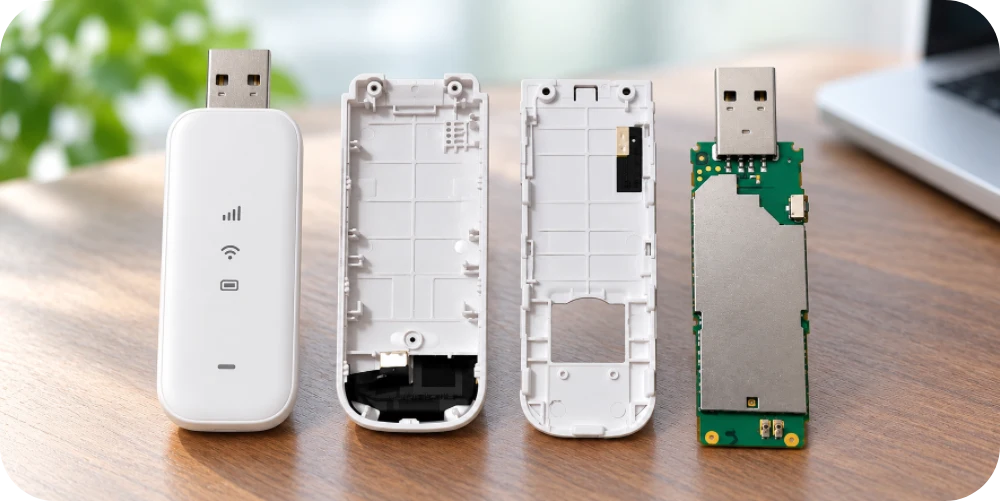
A Mobile Wi-Fi Router PCB is the production platform inside a battery-powered 4G/5G hotspot that combines cellular connectivity, Wi-Fi, SIM/eSIM support, power management, user interfaces and antennas in a compact enclosure. For an OEM, the manufacturing challenge is not simply whether the schematic works. The released board has to preserve RF behavior, charging performance, thermal margin and mechanical fit from the first engineering samples through later production lots.
Highleap Electronics is a PCB manufacturing and PCB assembly factory for customer-owned electronics. For mobile hotspot projects, our scope can cover bare PCB fabrication, component sourcing, SMT/THT assembly, shield and connector processing, programming, inspection and customer-defined functional test. We support prototype, pilot and volume orders, with quality controls and international B2B shipment built into the manufacturing plan.
This page is written for hardware teams that already own the product architecture and need a factory that can turn that design into repeatable PCBAs. The most useful RFQ therefore starts with the actual modem/Wi-Fi platform, regional SKU plan, stack-up, BOM, enclosure constraints and test requirements—not a generic “router board” description.
- Customer-designed bare PCB fabrication for prototype, pilot and production quantities.
- Turnkey or partial-turnkey PCBA with BOM sourcing, SMT/THT, shielding hardware and programming according to released instructions.
- Quality control that can include electrical test, AOI, X-ray for hidden joints and customer-defined functional/RF checks.
- Prototype builds for design validation, followed by controlled volume ramp without changing the manufacturing baseline unnecessarily.
- International packing and shipment for OEM, telecom, IoT and networking customers.
Manufacturing a Mobile Hotspot Starts With the Cellular/Wi-Fi Architecture
Mobile Wi-Fi Router Product Family: Pocket Wi-Fi, 4G Hotspots and 5G Hotspots
Mobile Wi-Fi Router PCB projects usually come from teams developing a portable cellular hotspot rather than a general home router. Common product forms include pocket Wi-Fi devices with a small display, compact hotspots with only LEDs and buttons, battery-powered routers for field teams, and 4G or 5G hotspot products that provide Wi-Fi to phones, tablets, laptops or embedded equipment. Some designs also expose Ethernet, USB tethering or external antenna connectors, but those features are optional rather than defining requirements.
The cellular side may be built around an approved modem module or a more integrated platform. Highleap’s 5G communication PCB manufacturing guidance is relevant when the product uses high-speed cellular hardware, while cellular IoT module integration is more directly related to designs built around pre-certified modem modules. The choice affects RF routing, component sourcing, firmware control, shielding, manufacturing test and certification strategy.
Adjacent products should be kept distinct. A fixed wireless CPE may use mains power, external antennas and Ethernet ports. A travel router may work mainly from Ethernet or an upstream Wi-Fi connection. A USB modem is usually a host-attached data peripheral without a local Wi-Fi access point. A cellular gateway can add industrial I/O or routing functions. These products share technologies, but the battery, RF and user-interface priorities of a pocket hotspot create a different manufacturing brief.
Mobile Hotspot vs Travel Router, USB Modem and CPE
| Product variant | Device-level role | PCB implication |
|---|---|---|
| 4G pocket hotspot | Portable LTE WAN shared over Wi-Fi | Cellular RF, Wi-Fi, SIM, battery and compact enclosure integration |
| 5G mobile hotspot | Higher-rate cellular WAN and local Wi-Fi | Potentially higher thermal density, RF complexity and power demand |
| Hotspot with Ethernet | Cellular router plus wired LAN | Adds Ethernet PHY/magnetics/connector and chassis constraints |
| Hotspot with USB tethering | Wi-Fi plus host data/power connection | Requires a defined USB data and power role, not merely a Type-C receptacle |
Mobile Hotspot Architecture: Cellular Modem, SIM, Wi-Fi and System Control
A practical hotspot architecture can be viewed as four interacting domains: cellular WAN, local Wi-Fi, system control and power. The cellular domain contains the modem or modem module, SIM or eSIM circuitry, RF front end and cellular antennas. The local wireless domain contains the Wi-Fi/Bluetooth radio or combo device, its RF matching network and antennas. System control may be integrated into the main SoC or distributed across a modem platform and auxiliary MCU. Power circuitry converts battery or USB input into multiple rails and controls charging, shutdown and protection.
The PCB layout must keep these domains electrically connected without allowing one to disturb another. High-speed digital interfaces between modem, processor and memory can inject noise into RF regions. Switching regulators can generate harmonics near radio bands. Display and LED circuits can create periodic noise. The RF PCB requirements for IoT and 5G devices therefore need to be interpreted in the context of the actual modem, frequency plan and antenna implementation rather than applied as a generic layer-count rule.
SIM access is another device-level concern. A removable SIM tray has mechanical alignment, ESD and insertion-cycle implications; eSIM removes the tray but changes provisioning and sourcing. Buttons, battery connectors, USB-C and any external antenna jacks must align with the enclosure. If the industrial design changes late, these mechanically fixed interfaces can force a PCB revision even when the schematic remains unchanged.
Architecture rule
Do not describe every mobile hotspot as a single-chip router. Some products use cellular modules, some use highly integrated platforms, and others partition functions across several ICs or boards. The released schematic and mechanical package are the manufacturing source of truth.
For an RFQ, Highleap does not need a marketing name such as “5G pocket Wi-Fi” to guess the architecture. We need the actual Gerber/ODB++ package, BOM, assembly data, modem and Wi-Fi platform, regional band population, antenna interfaces, mechanical constraints and target quantities. That lets the engineering team review manufacturability before material is committed. If the design is still in EVT or early DVT, rapid PCB prototyping can be used to validate the board before a larger buy.
RF Coexistence and Antenna Placement Can Decide First-Pass Yield
Cellular and Wi-Fi RF Design Inside a Portable Router
The most product-specific part of a mobile hotspot is the coexistence of cellular and local Wi-Fi radios in a very small enclosure. Antenna efficiency depends not only on the antenna component but also on ground geometry, feed routing, matching networks, enclosure plastics, battery placement, display metalwork and the user’s hand. PCB work should therefore follow the approved RF layout and antenna vendor or RF-engineering constraints instead of treating the antenna as an isolated footprint.
Useful background includes PCB antenna layout principles and radio antenna efficiency factors. In production, critical controls include feed-line geometry, matching-component values, shield-can land patterns, RF connector placement where present, antenna keep-outs and the exact stack-up used for impedance-sensitive traces. Substituting a matching capacitor or moving a shield frame can change RF behavior even when the part appears electrically similar on a BOM.
Coexistence also matters at the system level. Cellular transmit bursts, Wi-Fi transmit activity, USB traffic and switching regulators can interact. The design team may use filtering, shielding, spacing, synchronized control or firmware policies to manage these effects. Manufacturing must preserve those choices. A supplier should not “improve” copper pours, add test pads to an RF feed or change shield-can clearances without engineering review.
Practical Design Checklist
- Freeze antenna keep-out regions in the mechanical release.
- Control RF matching networks by exact approved MPN or engineering-approved alternate.
- Treat shield frames and spring contacts as electrical parts, not just mechanical accessories.
- Include final-enclosure RF checks in validation because open-board RF measurements cannot represent every user condition.
RF Stack-Up, Shielding and Mobile Wi-Fi Router PCB Fabrication
The PCB construction should be derived from routing density and electrical requirements rather than from a fixed “mobile router” recipe. A compact board may need multiple signal and reference layers for modem, memory, Wi-Fi, USB and power routing. Controlled-impedance structures can be required for RF feeds and high-speed digital interfaces. HDI may be justified around fine-pitch packages or very dense breakouts, but it should not be claimed as mandatory for every mobile hotspot.
RF isolation often combines layout and hardware shielding. RF shielding in production also requires that shield-frame pads must remain flat and solderable, covers must fit the mechanical stack, and ground stitching or enclosure contacts must match the released design. Fabrication changes in dielectric thickness or copper can affect impedance, while registration or solder-mask changes can affect dense RF packages.
DFM should also examine panelization, antenna keep-outs, board-edge connectors, SIM trays and any thin necks created by enclosure geometry. Bare-board electrical testing verifies continuity and shorts but cannot prove RF performance. The manufacturer should therefore separate fabrication controls from later RF and functional tests instead of implying that a passed electrical test guarantees a working hotspot.
For production release, the stack-up review should be linked to the antenna and modem reference files rather than treated as an isolated fabrication exercise. If the board house proposes a different core/prepreg combination, finished copper or via construction, engineering should re-check RF feeds and any high-speed channels before approval. It is also useful to identify which dimensions are electrically controlled and which are only mechanical, because that prevents unnecessary cost while protecting the parts of the design that influence RF and digital performance. Coupon requirements, impedance reports and material substitutions should be recorded with the hardware revision so a repeat order does not silently drift from the qualified build.
A good RF layout can still lose margin if stack-up, dielectric choice, copper geometry, connector launch, shielding-can flatness or assembly residue drifts between lots. Our job as the manufacturer is to hold the released construction and process windows consistently. For designs that require conducted checks, coupling fixtures or other production screening, RF PCB testing options can be incorporated into an agreed test flow rather than treated as a vague “RF test” line item.
Battery, USB Power and Thermal Limits Need Production Margins
Battery, Charging, USB-C and Thermal Design for Mobile Hotspots
Portable hotspots are energy-limited products. Battery capacity, modem activity, Wi-Fi load, display brightness, standby policy and cellular signal conditions all affect runtime. The PCB usually contains battery charging, protection or power-path circuitry plus several point-of-load rails. Highleap’s intelligent power-management PCB concepts and battery-management PCB considerations are relevant references, but the correct architecture depends on the customer’s cell pack, charging specification and system power tree.
USB-C deserves precise wording. A Type-C receptacle does not by itself prove a particular USB data generation, USB Power Delivery profile or charging power. The port role, CC/PD controller, charger, cable expectations and protection network must be defined by the product design. From a manufacturing perspective, the connector also experiences repeated insertion forces, so pad geometry, shell anchors, board edge location and enclosure support deserve DFM attention.
Thermal behavior can become important in 5G or weak-signal operation because modem and RF power stages may dissipate more heat while the product is enclosed and battery powered. Copper spreading, thermal vias, graphite or mechanical spreaders, shield cans and the chassis can all participate. A PCB manufacturer can preserve copper and via structures, but it cannot guarantee finished-device skin temperature without the final thermal stack, firmware and use case. Thermal validation should therefore be performed on complete assemblies under defined traffic and charging conditions.
Conversion point
For a useful quotation, provide the released stack-up, modem/platform BOM, antenna notes, battery/charger requirements, enclosure drawing and expected test scope. Those inputs reveal more manufacturing risk than the label “5G hotspot” alone.
Battery-powered hotspots often fail during scale-up because the board, battery pack and enclosure were validated separately. Charger current, modem transmit bursts, USB-C input limits, thermal pads and enclosure heat spreading should be documented together. Highleap can manufacture the released power design and coordinate assembly details; our battery-management PCB considerations resource is useful when reviewing how battery-related circuitry interacts with the main PCBA.
From Bare PCB to Assembled Hotspot PCBA at Highleap
PCBA Assembly, Component Sourcing and Variant Control for Hotspot Products
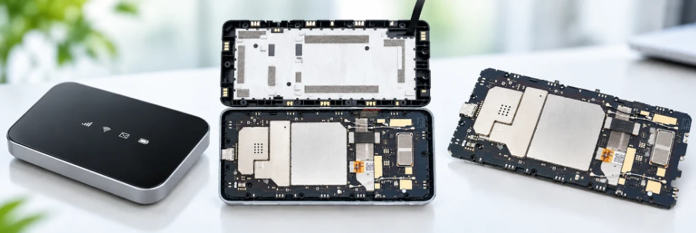
Mobile hotspot PCB assembly combines fine-pitch digital devices, RF components, power-management parts, connectors and often shield frames on a compact board. The communication PCB assembly process is relevant because placement accuracy, solder paste control and handling must work across components with very different package sizes and thermal masses. Hidden-joint packages may justify X-ray based on package risk, while AOI remains useful for visible solder and placement conditions.
Sourcing discipline is particularly important for modem platforms, RF front-end parts, oscillators, PMICs, memory and approved wireless modules. A substitution that matches package and headline value can still change RF bands, firmware, power behavior or certification status. Production should therefore use customer-approved manufacturer part numbers and a formal alternate approval path.
- Variant control becomes critical when one PCB supports regional SKUs. Different cellular band populations, SIM options, antenna configurations, memory sizes or labels may share the same bare PCB. The build package should link each SKU to a BOM, firmware image, calibration data, label and test profile. This prevents a geographically correct enclosure from receiving the wrong RF population or software image.
- A hotspot production line also needs a deliberate sequence for shield frames, thermal materials, SIM hardware and any hand-installed connectors. These operations can occur after primary SMT and may require dedicated fixtures or inspection. Before volume production, the team should define which parts are customer-consigned, which alternates require approval, how regional BOM variants are labeled and whether calibrated RF data follows the modem module or the finished unit. That manufacturing definition is especially valuable for 4G/5G products because one visually similar assembly can contain different RF populations. Procurement can then compare quotations on the same controlled scope instead of mixing bare-board, PCBA and regional-configuration costs.
For a turnkey build, Highleap can combine bare-board fabrication with controlled electronic component sourcing, solder paste printing, SMT placement, reflow, THT where required, inspection and customer-defined programming. The commercial advantage is fewer handoffs between the PCB house, component buyer and assembler. See our PCB assembly capabilities for the broader assembly scope.
Prototype Builds Should Retire the Highest-Risk Interfaces First
A 5–20 piece engineering build is optimized for learning: quick DFM feedback, controlled substitutions only with approval, and enough units for RF, firmware, battery and enclosure validation. A pilot run adds fixture readiness, traceability, work instructions and a more realistic yield picture. A volume program then focuses on material continuity, process capability, test throughput, packaging and change control.
Highleap can keep the same project moving through those stages. When demand is proven, high-volume PCB assembly provides the production framework for higher throughput while keeping the approved process matched to the actual hotspot design.
What to Test Before a Mobile Hotspot PCBA Leaves the Factory
Functional, RF and Battery Validation Before Shipment
A mobile hotspot that powers on is not necessarily production-ready. Verification can include firmware programming, SIM detection, cellular registration on an approved test setup, Wi-Fi SSID operation, client connection, data transfer, USB/charging behavior, display or LED checks, button inputs, battery current and thermal observation. The exact sequence should be supplied or approved by the customer because network credentials, firmware and acceptance thresholds are product-specific.
RF validation can range from fixture-based checks to conducted measurements or chamber work depending on the production plan. Highleap’s RF PCB test considerations are relevant to defining what is actually measured. A production factory should not claim carrier acceptance or regulatory certification merely because it performs RF functional tests; those are separate qualification activities.
- Battery tests also need clear limits. Charge current, cutoff behavior, standby draw and load current may be monitored, but the fixture must match the intended battery and firmware state. For repeat production, store test-software versions and golden-unit references with the hardware revision so later batches are compared against the correct configuration.
- A good end-of-line test should also reproduce the user path: power the unit from its intended source, verify boot and battery status, connect at least one Wi-Fi client, exercise the supported WAN path and confirm the correct regional firmware/configuration. For devices with a display, temperature sensor or Ethernet option, those functions should be checked only when fitted. Throughput testing does not need to become a lengthy benchmark on every unit; a shorter customer-defined data-transfer screen can detect assembly faults, while deeper RF and thermal characterization can remain a design-qualification or sampling activity. Separating these layers keeps production test economical without pretending that a simple connectivity check proves full product compliance.
The test boundary should be written into the quotation. Bare boards can be electrically tested; assembled boards can receive AOI and X-ray where package type calls for it; functional checks can cover boot, USB, indicators, charging, Wi-Fi association and customer-defined modem behavior. Carrier certification, regulatory approval and final antenna certification remain separate from routine factory screening unless specifically contracted and supported by the required equipment.
Cost, Regional SKUs and Supply Continuity
For mobile hotspots, the largest quote differences are usually not caused by the phrase “router PCB.” They come from layer count and via technology, controlled-impedance requirements, RF laminate use where actually necessary, modem/RF BOM value, shield cans, fine-pitch packages, antenna/RF connectors, programming, test time and quantity.
To receive a useful quotation, send: Gerber or ODB++, fabrication drawing and stack-up, BOM with manufacturer part numbers, pick-and-place, assembly drawing, approved substitute rules, regional SKU matrix, firmware/programming instructions, test requirements, mechanical files and target quantities. State whether you need PCB only, PCBA, or a wider box-build scope.
A Production Handoff That Can Survive the Next Order
A mobile hotspot is ready for production only when the approved hardware baseline is unambiguous. That baseline should identify the released PCB revision, stack-up and impedance requirements, approved BOM and alternates, modem/Wi-Fi firmware, regional population options, antenna and enclosure dependencies, labeling rules, programming data and the exact pass/fail limits used at final test.
Highleap can use prototype and pilot quantities to expose assembly or test issues before material is committed for a larger lot, then carry the approved process into repeat production. The value for an OEM is continuity: the next order should not require the factory to rediscover which shield, connector, firmware image or regional BOM was accepted on the last build.
For a production-ready quotation, send the Gerber/ODB++ data, fabrication notes, BOM with manufacturer part numbers, pick-and-place, assembly drawings, modem/Wi-Fi platform details, mechanical files, programming package, test procedure and target quantities. The objective is not just to quote one batch—it is to establish a controlled manufacturing baseline that can survive the next order.

Recommended Posts

TMM4 Filter PCB Manufacturing
TMM4 filter PCB manufacturing is controlled by the...

TMM3 PCB Manufacturing for RF Modules
TMM3 PCB manufacturing is most useful where the RF module...

TMM6 PCB Fabrication
TMM6 fabrication is the process-control page for a mid-Dk...

TMM10 PCB Manufacturing for Compact RF Designs
Table of contentsHow TMM10 Shrinks RF StructuresTMM10 vs...
How to get a quote for PCBs
Let’s run DFM/DFA analysis for you and get back to you with a report. You can upload your files securely through our website. We require the following information in order to give you a quote:
-
- Gerber, ODB++, or .pcb, spec.
- BOM list if you require assembly
- Quantity
- Turn time
For PCBA services, please provide your BOM (Bill of Materials) and any specific assembly instructions. We also offer DFM/DFA analysis to optimize your designs for manufacturability and assembly, ensuring a smooth production process.