
RO3010 PCB Manufacturing
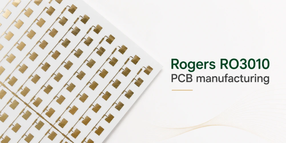
RO3010 fabrication is distinguished by the compact geometry enabled by a high-Dk construction. The manufacturing review therefore concentrates on dielectric thickness, trace and gap control, drilling, registration and impedance verification for the finished microwave board.
Figure 1. Rogers RO3010 PCB manufacturing
RO3010 PCB manufacturing is a compact-circuit problem. The higher-Dk construction can reduce the physical size of RF features, but the design becomes more sensitive to dielectric thickness, copper geometry and registration. Rogers RO3010 PCB manufacturing is chosen when a microwave circuit needs strong miniaturization from a Dk 10.2 ceramic-filled PTFE laminate. RO3010 has process Dk 10.2 +/- 0.30 and dissipation factor 0.0022 at 10 GHz. It can reduce filter, coupler, resonator, and antenna area, but the same high dielectric constant makes trace width, dielectric thickness, routing tolerance, drill quality, and final inspection more sensitive.
Table of Contents
Material scope: the Rogers product name is used to identify the laminate specified for the PCB build. Highleap Electronics provides PCB fabrication and assembly, while the laminate is sourced and verified separately.
When RO3010 Is the Right PCB Material
RO3010 is chosen when a microwave circuit needs high dielectric constant for significant size reduction. It is used in compact filters, couplers, resonators, antennas, power dividers, and RF modules where Dk 10.2 allows shorter electrical structures and denser layouts than lower-Dk laminates.
The tradeoff is that miniaturized RF geometry gives the fabricator less tolerance margin. Before quoting, the design should confirm finished copper, dielectric thickness, etched trace width, spacing, annular ring, connector launch geometry, and any frequency-critical copper pattern. This prevents a compact RF design from becoming difficult to reproduce.
High-Dk Miniaturization Makes DFM the Main Risk
RO3010 can make RF circuits much smaller, but that size reduction compresses the manufacturing window. Trace widths, gaps, annular rings, solder mask dams, and routed features may become small enough that normal tolerance assumptions are no longer acceptable. The board may have only a few layers, but it should still be reviewed like a precision microwave part.
The core topic is manufacturable miniaturization. Highleap checks whether the proposed trace geometry can be etched repeatably, whether the selected copper weight will push traces outside the model, whether drilled holes have enough annular ring, and whether connectors or shields create assembly constraints. On high-Dk boards, a small change in etched trace width or dielectric thickness can have a larger practical effect because the RF geometry is already compact.
An RO3010 RFQ should avoid sending only Gerbers and a material name. The RFQ quote should identify dielectric thickness, copper profile, finished copper target, impedance or frequency-sensitive features, coupon method, and any connector launch requirement. If the board contains filters, couplers, resonators, or antenna matching structures, those features should be marked as critical so engineering does not treat them as ordinary copper shapes.
- Confirm that compact traces, gaps, and annular rings are inside the supplier’s repeatable process window.
- Control copper weight and etch compensation because they directly affect small RF geometry.
- Identify critical RF structures on the drawing so inspection focuses on the features that matter.
RO3010 High-Dk Properties That Set Finished Geometry
| Item | Manufacturing meaning |
|---|---|
| Process Dk | 10.2 +/- 0.30 at 10 GHz, enabling strong circuit miniaturization. |
| Dissipation factor | 0.0022 at 10 GHz, suitable for compact microwave circuits. |
| High-Dk sensitivity | Small dimensional changes can shift RF behavior more noticeably. |
| Inspection priority | Coupons, microsections, and dimensional checks should match product risk. |
DFM and Stackup Review Before Quoting
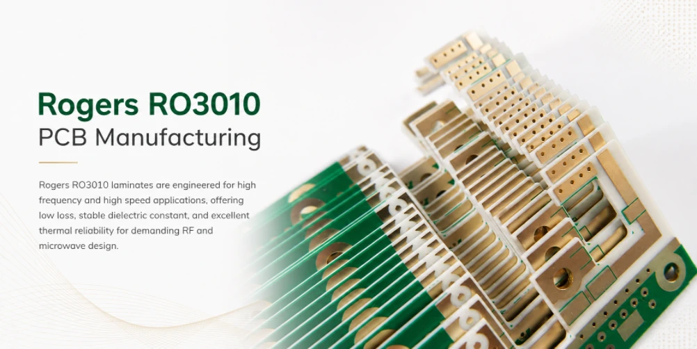
A reliable quote starts with the complete Gerber set, drill files, netlist, board outline, stackup drawing, material callout, copper weight, surface finish, solder mask notes, impedance targets, and any assembly requirements. Highleap checks whether the design can be fabricated repeatably before tooling starts.
| DFM item | What to check |
|---|---|
| Compact features | Check minimum trace/space, annular ring, solder mask dams, and routing clearance. |
| Stackup release | Confirm dielectric thickness, copper weight, finish, and impedance assumptions before quoting. |
| Assembly interface | Review RF launches, connectors, shields, thermal interfaces, and test access. |
Manufacturing Process Controls
The process route should be selected before material is released to production. Typical controls include material verification, inner layer inspection, lamination review, drill quality, hole-wall preparation, copper plating, solder mask registration, surface finish, routing accuracy, electrical test, and final inspection. Highleap reviews the finished stackup and RF line dimensions before CAM. For small filters, couplers or resonant structures, the fabrication drawing should make the finished geometry explicit because nominal layer thicknesses do not fully describe the RF result. Exact material property values should be checked against the current supplier documentation for the specified grade and construction.
For repeat miniaturized RF builds, keep the approved construction, copper target, panel format and RF inspection method stable. A small process change that is acceptable on a conventional board can shift a compact RO3010 feature enough to require RF re-tuning.
RFQ Package and Production Records
RO3010 is suited for miniaturized microwave filters, compact couplers, patch antennas, resonators, RF front-end modules, and dense hybrid assemblies where board area is limited and repeatable geometry is critical.
Send Gerber data, drill files, netlist, board outline, RO3010 thickness, copper weight, impedance targets, finish, solder mask, coupon notes, test needs, quantity, delivery schedule, and assembly files when turnkey PCBA is needed.
For RO3010 builds, useful evidence includes dimensional inspection of compact RF features, impedance verification, microsections where required, material records and electrical test. First-article results are especially useful when the design contains very small filters, couplers or resonant features. For quotation, provide the exact construction, finished thickness, copper, frequency band, impedance requirements and quantity. A complete drawing allows the manufacturer to judge whether the desired miniaturization fits the production process.

Recommended Posts

TMM4 Filter PCB Manufacturing
TMM4 filter PCB manufacturing is controlled by the...

TMM3 PCB Manufacturing for RF Modules
TMM3 PCB manufacturing is most useful where the RF module...

TMM6 PCB Fabrication
TMM6 fabrication is the process-control page for a mid-Dk...

TMM10 PCB Manufacturing for Compact RF Designs
Table of contentsHow TMM10 Shrinks RF StructuresTMM10 vs...
How to get a quote for PCBs
Let’s run DFM/DFA analysis for you and get back to you with a report. You can upload your files securely through our website. We require the following information in order to give you a quote:
-
- Gerber, ODB++, or .pcb, spec.
- BOM list if you require assembly
- Quantity
- Turn time
For PCBA services, please provide your BOM (Bill of Materials) and any specific assembly instructions. We also offer DFM/DFA analysis to optimize your designs for manufacturability and assembly, ensuring a smooth production process.