
mSAP PCB Manufacturing for Fine-Line Circuitry
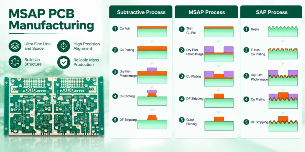
Highleap Electronics provides mSAP PCB manufacturing review and quotation for fine-line circuit designs where the required conductor geometry, pitch and copper construction call for a modified semi-additive process. If your current supplier cannot support the specified line width, spacing or fine-pitch layout, send us the released artwork and stackup so the process requirements can be assessed against the actual design.
For mSAP PCB fabrication, a minimum line/space number on its own is not enough. Finished conductor width, copper thickness, dielectric system, layer registration, impedance targets, panel layout and inspection criteria must be considered together. Highleap’s quotation process is intended to establish the required construction and confirm the process assumptions before price and delivery are committed.
Table of contents
The achievable line/space depends on seed copper, resist imaging, plated copper thickness, seed removal and inspection control.
mSAP PCB Manufacturing vs Subtractive Etching
A conventional multilayer board is built subtractively. The entire layer is covered in copper, an image is printed in dry film, the exposed copper is etched away, and the remaining copper is the pattern. The final line width is therefore the photolithography line width minus whatever the etch removes, and the etch is not vertical. It undercuts, and it does so unevenly depending on the copper thickness and the aspect ratio of the feature.
The semi-additive process reverses the logic. The pattern is first created as a thin seed layer in the shape of the desired features, and copper is then plated up to full thickness. Because copper is plated up from a thin seed layer, mSAP can reduce the lateral undercut associated with subtractive etching. Final line geometry still depends on imaging, resist profile, plated copper thickness, seed-layer removal and process control; it is not determined by lithography alone.
This is what makes mSAP different in practice. The finished copper is not defined by the etch. It is defined by the image, and then grown. That is why mSAP can produce fine-pitch pad arrays and narrow traces that a subtractive route would either round off or require an enormous amount of over-correction to survive the etch.
mSAP vs Standard PCB Fabrication for Fine-Line Designs
Because the seed layer has to be printed and the plating has to be uniform, mSAP on a conventional laminate is possible but is not the best route. The industry practice is to build mSAP structures on a material system whose surface chemistry supports the process: a very smooth copper foil, and in the highest-performance structures a resin system with low loss and good dielectric consistency.
| Factor | Subtractive on standard laminate | mSAP on dedicated laminate |
|---|---|---|
| Line width control | Defined by etch compensation; limited by foil roughness and copper thickness | Defined by the image; finer lines achievable at the same copper thickness |
| Sidewall profile | Undercut, worst on thick copper and high-aspect-ratio features | Near-vertical, which is what makes fine-pitch structures possible |
| Surface roughness | Etched foil surface, relatively rough | Smoothed as a byproduct of the plating and stripping cycle |
| Impedance accuracy | Width variation couples into impedance error, especially on thin dielectrics | Tighter width control supports tighter impedance tolerance |
| Process steps | Standard | Adds seed printing, selective plating, stripping and a second surface prep |
If the requirement is simply “fine lines” and not “fine lines with controlled impedance on a thin dielectric”, a conventional fine-line process on a high-grade laminate may meet the requirement at a lower cost. The case for mSAP becomes strong when the fine features are also dense, when the copper is thick relative to the line width, or when the geometry is genuinely at the limit of what photolithography and etching can resolve.
mSAP PCB Manufacturing Process for Fine-Line PCBs
The sequence below is the core of the process. Each step exists to prepare the surface for the next one, and the order is not flexible.
| Step | Process | Critical control |
|---|---|---|
| 1. Surface preparation | Micro-etch and roughening of the foil surface to give the seed layer adhesion | Uniform and reproducible. Under-etching causes the seed layer to lift; over-etching defeats the smoothing benefit |
| 2. Dry film or laser imaging | The desired feature pattern is formed in the imaging layer | Resolution and alignment. This is the step that sets the final line width |
| 3. Seed layer | A thin electroless copper layer is deposited over the whole surface and the imaging layer is stripped | Seed layer continuity and thickness. A discontinuity becomes a plating defect at exactly that point |
| 4. Selective plating | Copper is electroplated up to the full copper weight, only on the seed areas | Plating distribution across the panel. Uniform current distribution is what keeps the copper thickness and therefore the line width consistent across a large panel |
| 5. Strip and etch | The seed layer outside the features is stripped, then a light etch removes the residue | The etch is now only cleaning up, not forming the feature. This is the structural difference from subtractive processing |
| 6. Repeat per layer and laminate | The cycle is repeated on each inner layer, and the stack is pressed together | Registration between layers, and laminate compatibility with the finished copper surface |
Step 4 is where most of the difficulty sits. Electroplating is a panel-level process: the current distribution across a large panel is never perfectly even, so copper thickness varies, and where thickness varies the finished line width varies. Panel format and utilisation depend on the fabricator’s equipment, plating uniformity controls and the specific design. Finished board dimensions should therefore be included in the quote so the proposed panel layout and process route can be evaluated.
mSAP Fine Line and Space Requirements for PCB Fabrication
The plating bath in an mSAP line is not interchangeable with a general-purpose copper plating bath. Additives in the bath control the plating rate and the throwing power, and the behaviour that matters for mSAP is how the bath grows copper in narrow trenches between seed areas. A bath that plates well in an open area can starve the interior of a fine-pitch array, producing a taper or a gap between the pad and the trace.
Three consequences follow for the buyer, and they are worth understanding because they show up on the drawing review:
- Aspect ratio in the planar direction matters. A dense pad array behaves like a set of narrow trenches to the plater. The denser the array and the finer the pitch, the harder it is to plate uniformly, and the more the process depends on the fabricator’s specific chemistry and panel design.
- The seed layer is a bottleneck for fine structures. Electroless deposition in a fine space can be slow or incomplete. This is a real constraint on achievable feature size and it is not removable by better lithography.
- Thicker copper is disproportionately harder. Because the plating has to fill the space uniformly to the full copper weight, a heavy copper requirement on fine features is one of the most difficult combinations in this process.
The related subtractive route for dense structures is discussed in our laser direct imaging (LDI) process, and the drilling side of fine-pitch work in our laser-drilled PCB vias. For boards that combine fine lines with a build-up structure, the stackup question is covered in our HDI stackup design.
mSAP PCB Design Rules for Fine-Pitch Components
Designing for mSAP is not designing for standard photolithography with tighter numbers. Several rules change in kind rather than in value.
- Annular ring is no longer a minimum-width constraint. Because the copper grows rather than being etched, the pad can be close to the size of the finished hole without the undercut eating the pad away. This is what allows dense pad arrays, and it is a real gain in routable area on a fine-pitch design.
- Etch compensation is not needed in the same way. A designer accustomed to compensating for etch loss should re-check the design, because the finished feature is close to the imaged feature.
- Copper weight on fine features has to be justified. If the design asks for 2 oz copper on 50 µm lines, the plating step has to fill that uniformly and the process margin becomes thin. There is often a thickness-versus-width relationship worth reviewing before release.
- Impedance values must be recomputed for the finished copper. The characteristic impedance depends on the trace width and the copper thickness, and the mSAP copper surface is smoother than an etched one. If the impedance target was set from a standard process calculation, it is worth checking against the actual finished geometry.
Impedance control in general is discussed on our RF PCB impedance control and in the broader controlled-impedance PCB design, and the fine-feature consequences for RF layouts are covered in our RF PCB design guidelines.
When to Use mSAP Technology for High-Density PCBs
mSAP earns its cost in specific situations, and in others a conventional fine-line process on a better laminate is the rational answer. It pays when the design contains fine-pitch pad arrays that a subtractive route cannot resolve, when a trace’s width sets its impedance and the width tolerance is tight, when copper must be thick relative to the line width, and where a structure is dense enough that an ordinary board would need more layers than the mechanical design allows.
It does not pay when the only requirement is a modest reduction in line width, when the board is large and the copper weight is heavy but the features are ordinary, or when volume is high enough that the process cost dominates and a conventional process on a fine-line laminate gets within the required tolerance. In those cases, a HDI PCB manufacturing process with laser drilling and a high-grade laminate is usually the more sensible specification.
Material selection interacts with the decision more than buyers expect. The laminate has to be compatible with the seed layer chemistry, and for RF structures the dielectric constant and loss tangent of the resin system set the achievable performance regardless of how good the copper is. Our PCB material selection covers the trade-offs, and the low-loss material families specifically in our low-Dk and low-Df PCB materials.
mSAP PCB Cost and Lead Time for Fine-Line Manufacturing
On an mSAP quotation, the price is not primarily the copper. It is the process steps and the panel discipline.
- Number of imaging and plating cycles. Each inner layer in a build-up structure is a full mSAP cycle. A four-layer build-up on top of a core is four mSAP cycles, not one.
- Panel size. mSAP panels are smaller because plating uniformity degrades over large areas. A board that is not a good fit for a standard panel can cost considerably more purely for that reason.
- Yield on the fine structures. A defect on a dense array is more likely and more costly, because it is usually detected late and it can scrap a whole panel.
- Material. The laminate and copper foil specification carries a real premium, and it is a larger share of the cost on a fine-line board than on a conventional one.
- Measurement. Fine features need to be measured, and the measurement method is part of the quotation.
If the schedule is the constraint rather than the price, say so in the RFQ. A smaller panel, a simpler stackup, or splitting the build into two steps can each change the lead time materially, and the fabricator can only optimise for that if they know it matters. Lead time structure for these builds is set out in our PCB manufacturing process flow.
mSAP PCB Manufacturer for Fine-Line and Fine-Pitch Designs
When searching for an mSAP PCB manufacturer, engineers should compare verified process capability for the intended stackup—not just the smallest advertised line width. Highleap can review mSAP PCB fabrication enquiries involving fine-line routing, dense pad patterns and controlled copper geometry, then clarify which construction details and qualification checks are needed before a production commitment.
For a fine-line PCB manufacturing quote, provide the finished line width and spacing, copper thickness by layer, dielectric materials, stackup, layer count, board size, impedance requirements and expected volume. If the design targets fine-pitch pads or high-speed signals, include the footprint details and impedance table. These inputs help distinguish a design that requires mSAP from one that may be manufacturable through a conventional fine-line process at lower cost.
Where the design combines fine-line routing with high-density interconnects, Highleap’s HDI PCB manufacturing route may be relevant. For controlled impedance, include the requirements alongside the controlled impedance PCB design details. Use the Request a quote for fine-line PCB fabrication to submit the complete design package.
- Quote package: Gerber/ODB++ files, stackup, line/space targets, copper thickness, impedance table if applicable, inspection requirements and forecast volume.
mSAP PCB Manufacturing FAQs
Is mSAP the same as a build-up or sequential lamination structure?
No, they are different dimensions. Sequential lamination and build-up describe how the layers are stacked and pressed. mSAP describes how the copper image on a layer is formed. A board can be mSAP without being a build-up, and a build-up can be made by subtractive processing. They are often used together, which is why the terms get mixed up in enquiries.
What line width can mSAP actually achieve?
It depends on the copper weight, the material, the plating chemistry and the panel size. Rather than quote a headline number, the useful question is what the smallest feature is on your board, what copper weight it carries, and what the density around it is. Those three together determine whether the design is comfortable or marginal.
Can mSAP be used with blind and buried vias?
Yes. The via structures are formed by drilling and plating as in any build-up process, and the copper layers can be produced by mSAP. The interaction to watch is the plating of the via wall and the plating of the planar layer, since both happen in the same chemistry bath and the via must be plated in a way that does not trap contamination in the seed layer.
Does mSAP change the achievable layer count?
It changes the practical limit on a dense build-up, because each additional layer adds a plating cycle with its own yield risk. The mechanical and material limits still apply in parallel. A design that needs many layers and very fine features is usually better served by reviewing the layer count as a design variable.
Can the finished board be soldered and assembled normally?
Yes. mSAP affects the copper formation, not the assembly process. It is worth confirming that the surface finish is specified, since a fine-pitch board assembled on a surface that is not solderable is a common and avoidable problem.
mSAP PCB MANUFACTURING · RFQ
Request an mSAP PCB Manufacturing Review
Send the Gerber, stackup, minimum line width, minimum pad pitch, copper weight and finished board size. We confirm the process route and quote it with the mSAP steps included.
Min line width + min pitch + copper weight.

Recommended Posts
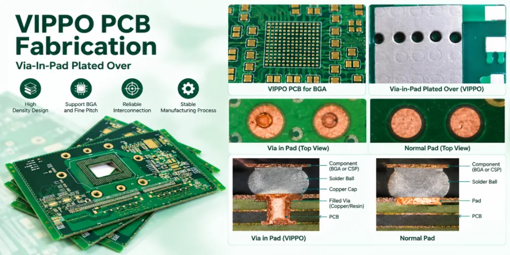
VIPPO PCB Fabrication for BGA and Thermal Pad Designs
Highleap Electronics provides VIPPO PCB fabrication for...
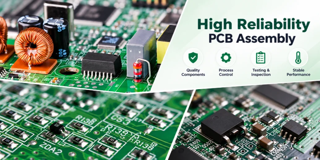
High Reliability PCB Assembly: Process Control and Traceability
Highleap Electronics manufactures high reliability PCB...
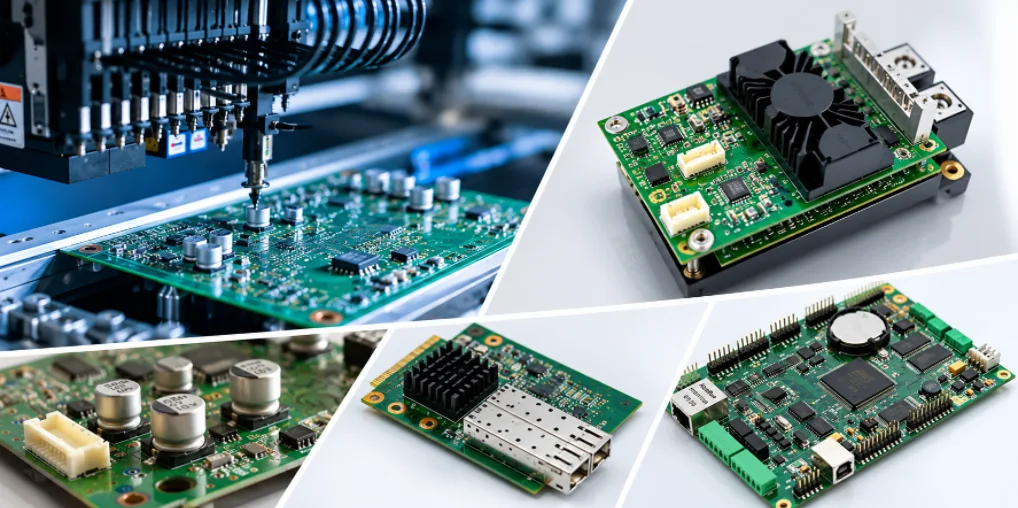
Expedited PCB Assembly: Lead Times, Readiness and Cost
Highleap Electronics offers expedited PCB assembly for...
Small-Batch High-Mix PCB Assembly for Repeat Orders
Highleap Electronics provides small-batch, high-mix PCB...
How to get a quote for PCBs
Let‘s run DFM/DFA analysis for you and get back to you with a report. You can upload your files securely through our website. We require the following information in order to give you a quote:
-
- Gerber, ODB++, or .pcb, spec.
- BOM list if you require assembly
- Quantity
- Turn time
In addition to PCB manufacturing, we offer a comprehensive range of electronic services, including PCB design, PCBA, and turnkey solutions. Whether you need help with prototyping, design verification, component sourcing, or mass production, we provide end-to-end support to ensure your project’s success.
For PCBA services, please provide your BOM (Bill of Materials) and any specific assembly instructions. We also offer DFM/DFA analysis to optimize your designs for manufacturability and assembly, ensuring a smooth production process.