
Laser direct imaging(LDI)in PCB manufacturing
 in PCB Manufacturing")
In the ever-evolving field of PCB manufacturing, the need for higher precision, smaller features, and greater circuit density has pushed manufacturers to adopt more advanced technologies. One of the most influential innovations in this area is Laser Direct Imaging (LDI), a process that has become essential in meeting the increasing complexity of electronic devices.
At Highleap Electronic, we embrace LDI technology to provide high-precision, cost-effective, and scalable PCB manufacturing solutions. This article explores how LDI works, the benefits it brings to PCB manufacturing, and why it is an essential tool for designing and producing the next-generation electronics.
What is Laser Direct Imaging (LDI)?
Laser Direct Imaging (LDI) is a cutting-edge technology used in PCB manufacturing to directly transfer circuit patterns onto the PCB surface using a focused laser beam. Unlike traditional photolithography, which uses photomasks to transfer circuit designs, LDI eliminates the need for physical masks, offering several advantages such as faster production times, improved accuracy, and greater design flexibility.
How LDI Works
The LDI process starts with digital files (such as Gerber data) that describe the circuit layout. A computer-controlled laser then traces this design onto the PCB surface by using light exposure to define the features, such as traces and vias. The laser system scans the surface of the board, creating high-resolution patterns that meet the exact specifications of modern, high-density PCB designs.
The Need for LDI in PCB Manufacturing
As the demand for smaller, faster, and more complex devices continues to grow, traditional PCB manufacturing methods are increasingly limited in their ability to meet these needs. Whether it’s in wearables, medical devices, or the fast-evolving 5G technology, these industries require high-precision PCBs with smaller components, finer traces, and high-density designs. Laser Direct Imaging (LDI) technology is now the go-to solution for overcoming the limitations of conventional photolithography methods. Here’s why LDI is the key to advancing PCB manufacturing:
1️⃣ Miniaturization of Devices
The continuous trend toward miniaturization in electronics means that devices must become smaller, lighter, and more power-efficient. In response, PCBs need to support smaller components and increasingly complex designs. LDI technology is essential in this transformation, allowing manufacturers to create extremely fine traces, down to a few micrometers. This precision is critical for developing compact devices such as smartwatches, implantable medical devices, and IoT sensors, where every square millimeter of space must be optimized for performance.
2️⃣ Increased Demand for HDI PCBs
As electronic devices become more compact and performance demands increase, the need for High-Density Interconnect (HDI) PCBs has surged. HDI boards are essential for devices that require higher circuit density and smaller electrical paths to reduce signal loss and improve overall performance. LDI technology is perfect for these advanced designs, offering unmatched precision to create microvias and small vias that are essential for high-density boards. This is particularly important for cutting-edge technologies like 5G, IoT, and medical electronics, where compact, high-performance circuits are needed to ensure reliable signal integrity and fast data transmission.
3️⃣ Rapid Prototyping and Faster Time-to-Market
In industries such as wearables, telemedicine, and consumer electronics, rapid prototyping is crucial for bringing innovative ideas to market quickly. LDI technology offers a significant advantage by eliminating the need for traditional photomasks. This allows for faster iterations, reduced lead times, and quicker production cycles, making it possible to test and modify designs with speed and efficiency. The flexibility provided by LDI enables companies to reduce time-to-market, ensuring that new devices can be launched faster, giving businesses a competitive edge in a fast-paced market.
At Highleap Electronic, we leverage Laser Direct Imaging to produce high-quality, high-precision PCBs for a variety of industries, ensuring your designs stay at the forefront of innovation. Whether you need HDI PCBs, flexible circuits, or rapid prototyping, LDI is the key to unlocking the potential of tomorrow’s devices.
Processes Enhanced by LDI Technology in PCB Manufacturing
Laser Direct Imaging (LDI) technology plays a pivotal role in advancing PCB manufacturing, offering unmatched precision, enhanced reliability, and greater efficiency across multiple processes. By eliminating the need for traditional photomasks, LDI enables the production of smaller, more complex designs that are essential for the miniaturization and performance demands of modern electronics.
1️⃣ Inner Layer Imaging
In multilayer PCBs, inner layer imaging is crucial for the accurate creation of intricate circuit patterns. LDI technology allows for high-precision patterning, essential for high-density interconnect (HDI) PCBs. It enables the creation of fine lines, microvias, and small features that are vital for ensuring the functional integrity of inner layers, especially as designs become more compact and feature-dense.
2️⃣ Outer Layer Imaging
The outer layers of a PCB require extremely fine traces and small vias to accommodate compact designs and high-frequency applications. LDI ensures high-precision patterning, which is necessary to achieve the narrow line widths and tight spaces that are critical for RF applications and miniaturized devices. This capability is key to meeting the increasing demand for high-performance electronics such as wearable tech, 5G devices, and medical equipment.
3️⃣ Solder Mask Application
Accurate application of the solder mask is essential for protecting the PCB and ensuring the quality of the soldering process. LDI enhances the precision of solder mask applications, enabling the exact definition of solder mask openings. This results in optimized performance, reduced short circuits, and increased reliability in the final product, which is especially critical for high-density, high-frequency PCBs used in mission-critical applications.
4️⃣ Silkscreen Layer Printing
Although the silkscreen layer (used for labeling and identification) does not directly affect the PCB’s functionality, LDI technology significantly improves the resolution and clarity of printed labels and markings. This enhancement results in clearer and more durable markings, which are crucial for proper identification and tracking of the PCB, as well as improving the aesthetics and quality control in the manufacturing process.
5️⃣ Rapid Prototyping
In rapid prototyping, speed and flexibility are essential for quickly testing and modifying PCB designs. LDI technology provides greater design flexibility by eliminating the need for physical photomasks, enabling faster iterations and reduced lead times. With LDI, design changes can be implemented immediately, allowing for quicker transitions from concept to prototype testing, thereby accelerating product development cycles.
6️⃣ High-Density Interconnect (HDI) Boards
As electronic devices become more compact and powerful, the need for HDI boards continues to grow. LDI is ideal for HDI PCBs, as it enables the creation of microvias, fine traces, and small vias with high precision. These advanced capabilities make LDI technology essential for high-speed circuits in mobile devices, wearables, and 5G infrastructure, where minimizing signal loss and enhancing circuit density are critical.
7️⃣ Flexible and Rigid-Flex PCBs
Flexible and rigid-flex PCBs present unique challenges due to their combination of flexibility and rigidity. LDI technology provides the high precision required to handle the complexity of these designs, ensuring that electrical integrity is maintained without compromising flexibility. This makes LDI ideal for producing flexible circuits used in wearable devices, medical implants, and other high-performance applications where flexibility and durability are paramount.

Advantages of Laser Direct Imaging (LDI) in PCB Manufacturing
Laser Direct Imaging (LDI) offers significant advantages over traditional PCB manufacturing methods, particularly when producing high-density, miniaturized, and complex PCB designs. The ability to create fine features and maintain high precision makes LDI an essential tool for meeting the evolving demands of industries such as telecommunications, medical devices, IoT, and consumer electronics. Below are the key benefits that LDI brings to PCB manufacturing:
✅ High Resolution and Precision
LDI systems enable micrometer-level resolution, which is essential for creating ultra-fine traces, small vias, and complex circuit patterns. This high precision makes LDI ideal for HDI PCBs, which require fine details and high-density interconnects (HDI) for advanced electronic applications. With the ability to create narrow traces and dense routing, LDI supports the development of devices such as smartphones, wearables, and 5G technology that demand compact and efficient circuit boards.
✅ Reduced Alignment Errors
One of the most critical factors in multilayer PCB manufacturing is precise layer alignment. Traditional photolithography processes can lead to alignment issues, resulting in misplaced vias or traces between layers. With LDI technology, these alignment errors are significantly reduced, ensuring that all layers are accurately registered. This is especially important for multilayer HDI boards, where the exact positioning of components is necessary to ensure the performance and reliability of high-speed circuits.
✅ Design Flexibility and Rapid Changes
With LDI, design modifications can be implemented immediately without needing to create new physical masks, significantly speeding up the design iteration process. This feature is particularly beneficial during the prototyping phase, where multiple design changes are often required. LDI’s flexibility enables manufacturers to make rapid adjustments to the design without incurring additional costs or delays associated with mask production. This accelerates product development and facilitates faster innovation cycles.
✅ Faster Production Times
Traditional mask creation can be time-consuming and labor-intensive. By eliminating the need for physical masks, LDI allows for faster production times, particularly beneficial for small-to-medium production runs or rapid prototyping. The streamlined process enables manufacturers to deliver products to market faster, reducing the overall time-to-market and providing a competitive advantage. This is especially crucial in industries where speed and agility are essential for success.
✅ Improved Yield and Consistency
With traditional photomask-based processes, there is always the risk of defects caused by mask misalignment or wear and tear over time. LDI technology eliminates these issues, resulting in higher yield rates and more consistent quality across production batches. The high precision provided by LDI ensures that every PCB meets strict performance standards, improving the overall reliability of the final product and reducing the likelihood of defects and failures during use.
✅ Cost-Effectiveness for Small Batches
For prototype production or small batch runs, LDI proves to be more cost-effective than traditional methods. Traditional PCB production often requires expensive photomasks that are costly to create and maintain. With LDI, there is no need for these physical masks, reducing upfront costs and eliminating the need for mask storage. This makes LDI an ideal choice for companies needing rapid prototypes or small production runs where the cost of traditional mask creation would be prohibitive.
✅ Environmental Sustainability
The use of LDI technology not only improves efficiency but also makes the PCB manufacturing process more environmentally sustainable. Traditional PCB manufacturing generates waste from mask production and mask disposal, which can contribute to material waste. With LDI, the elimination of physical masks reduces the overall material consumption and waste generation, making it a more eco-friendly option. By adopting LDI, companies can contribute to more sustainable manufacturing practices while also maintaining high levels of precision and performance.
Why LDI is a Game-Changer in PCB Manufacturing
The introduction of Laser Direct Imaging (LDI) has revolutionized the way PCBs are manufactured. Offering unparalleled precision, flexibility, and cost efficiency, LDI has become a cornerstone of modern PCB production, particularly for industries that demand high-density, complex designs. As electronics continue to shrink and performance expectations rise, LDI technology ensures that manufacturers can meet these demands while improving yield, efficiency, and sustainability.
At Highleap Electronic, we leverage LDI technology to provide high-precision PCB solutions for a wide range of industries, from medical devices to telecommunications. By integrating LDI into our manufacturing process, we ensure that our customers receive the best quality, reliability, and cost-efficiency for their PCB designs.
Contact Us Today to Learn More About LDI in PCB Manufacturing
📩 Reach out to us for a free consultation and quote to discover how Laser Direct Imaging can optimize your PCB production and help bring your innovative designs to life!
FAQ: Laser Direct Imaging (LDI) in PCB Manufacturing
1. How does LDI address signal integrity challenges in high-frequency PCBs (e.g., 5G/mmWave)?
LDI’s micron-level precision ensures consistent trace widths and spacing, minimizing impedance variations that cause signal reflections. For 28+ GHz designs, it achieves <5 μm trace resolution, critical for maintaining phase coherence in RF circuits. Highleap pairs LDI with TDR testing to validate impedance (±2% tolerance) and insertion loss (<0.2 dB/cm) in 5G antenna arrays.
2. What environmental waste reduction does LDI offer compared to traditional photolithography?
By eliminating photomasks, LDI reduces chemical waste from mask cleaning and physical waste from outdated masks. For a 1,000-board batch, this cuts solvent use by 30–40% and avoids 15–20 kg of acrylic/polyester mask waste. Highleap further enhances sustainability via dry film resist recycling.
3. Can LDI handle advanced HDI structures like staggered microvias or skip-vias?
Yes. LDI’s 5 μm laser spot size enables precise drilling of staggered 50 μm microvias and skip-vias in 20-layer HDI boards. This supports 0.2 mm pitch BGAs in AI accelerators, with 99.9% via registration accuracy via AOI post-inspection.
4. How does LDI improve reliability for flexible PCBs in wearable devices?
LDI’s maskless process avoids mechanical stress from mask alignment on flexible substrates like polyimide. It achieves 25 μm traces on flex-rigid designs while maintaining >90% yield, essential for foldable electronics and medical wearables exposed to bending cycles.
5. What design file standards are required for LDI compatibility?
LDI supports standard Gerber X2 or ODB++ formats, but Highleap recommends including impedance profiles and layer-specific DRC rules in the files. For ultra-fine features (e.g., 3/3 mil traces), vector-based formats ensure smoother edge definition than rasterized data.
6. Does LDI limit material choices for high-Tg or specialty substrates?
No. Highleap’s LDI systems are compatible with high-Tg FR-4 (Tg=180°C), Rogers RO4000, and polyimide. The laser wavelength (355 nm) is optimized for low-Df materials, ensuring <1% CD variation even on low-CTE aerospace laminates.
Get a Free PCB & PCBA Quote

Recommended Posts
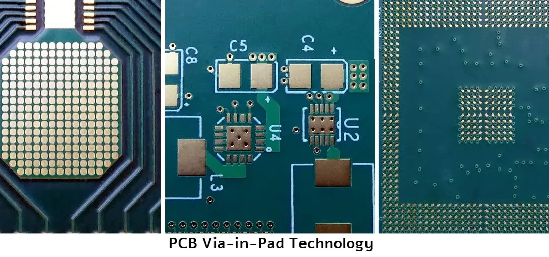
Comprehensive Analysis of PCB Via-in-Pad Technology
[pac_divi_table_of_contents...

PCB Hole Selection to Optimize PCB Performance and Cost
[pac_divi_table_of_contents...

Best Practice Guide for Slots and Cutouts in PCB Manufacturing
[pac_divi_table_of_contents title="On this article"...

Comprehensive Guide to Plated Through-Hole (PTH) Technology in PCB Manufacturing
[pac_divi_table_of_contents title="On this article"...
How to get a quote for PCBs
Let us run DFM/DFA analysis for you and get back to you with a report.
You can upload your files securely through our website.
We require the following information in order to give you a quote:
-
- Gerber, ODB++, or .pcb, spec.
- BOM list if you require assembly
- Quantity
- Turn time
In addition to PCB manufacturing, we offer a comprehensive range of electronic services, including PCB design, PCBA (Printed Circuit Board Assembly), and turnkey solutions. Whether you need help with prototyping, design verification, component sourcing, or mass production, we provide end-to-end support to ensure your project’s success. For PCBA services, please provide your BOM (Bill of Materials) and any specific assembly instructions. We also offer DFM/DFA analysis to optimize your designs for manufacturability and assembly, ensuring a smooth production process.