
SDR Vector Signal Generator PCBA: RF PCB Design and Assembly Considerations

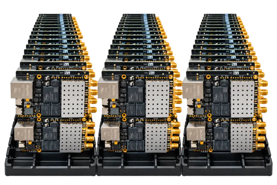
An SDR vector signal generator brings digital processing, frequency synthesis, high-speed conversion, RF signal conditioning, power management, and communication interfaces together on a single electronic assembly. At this level of integration, the PCB is part of the signal path and power architecture—not simply a platform for mounting components.
That distinction becomes important when an SDR design moves from engineering release to production. The PCB may require controlled impedance, a defined stackup, dense BGA or fine-pitch packages, closely positioned RF components, and specific inspection or functional-test requirements. The manufacturing process needs to reproduce those requirements consistently without introducing unnecessary variation.
For engineers and purchasing teams sourcing an SDR Vector Signal Generator PCBA, the key considerations therefore extend from PCB fabrication and RF layout through component assembly, DFM, inspection, and final verification.
Highleap Electronics supports PCB fabrication and PCB assembly based on customer-supplied engineering data, including PCB files, BOMs, assembly documentation, and defined production requirements.
—
What Defines a Reliable SDR Vector Signal Generator PCBA?
An SDR vector signal generator PCBA brings several demanding circuit functions together on one assembly. Digital processing, high-speed data conversion, frequency generation, RF amplification, filtering, attenuation, power management, and communication interfaces can all have different layout and manufacturing requirements.
The important manufacturing question is not simply whether every component is populated. The finished PCBA needs to preserve the electrical relationships established in the released design.
For example, an FPGA or processor may require high-density BGA assembly, while ADC and DAC devices depend on clean high-speed signal paths and stable power delivery. RF amplifiers, filters, attenuators, and frequency-generation circuits are sensitive to layout geometry, grounding, component selection, and signal-path continuity.
A reliable production process therefore needs to keep several areas aligned:
- PCB construction and approved stackup
- RF routing and controlled-impedance requirements
- Component selection and approved manufacturer part numbers
- High-density SMT assembly
- Soldering and reflow process control
- Inspection and hidden-joint verification
- Electrical, functional, and RF testing
This integrated approach is particularly important when the same design needs to move from prototype quantities into repeat production.
For projects requiring both bare PCB fabrication and component assembly, see PCB Assembly.
RF PCB Layout, Stackup, and Signal Integrity Considerations
RF performance is closely connected to the physical PCB structure. Controlled impedance depends on factors such as dielectric thickness, copper thickness, trace width, reference-plane configuration, and the actual fabricated stackup.
For a 50-ohm RF path, the impedance requirement should therefore be treated as a manufacturing requirement as well as a PCB layout requirement. The fabricated board must reproduce the geometry and layer structure used by the engineering design.
Several details deserve attention during PCB manufacturing:
- Controlled-impedance traces: Trace geometry needs to match the approved stackup and impedance target.
- Reference planes: Continuous reference structures help maintain predictable high-frequency return paths.
- RF vias: Layer transitions can introduce discontinuities and should follow the released layout.
- Connector transitions: RF connector launches can influence the transition between the PCB and external equipment.
- Ground structures: Grounding and return-current paths should remain consistent with the intended RF architecture.
- Component placement: Frequency-generation devices, converters, filters, amplifiers, attenuators, and RF connectors should remain positioned according to the released signal-path design.
For additional engineering considerations, see RF PCB Design and RF PCB Impedance Control.
The manufacturing objective is not to redesign the RF circuit during production. It is to reproduce the specified PCB construction and geometry consistently and to identify manufacturability risks before they affect the build.
High-Density Component Assembly for SDR Hardware
SDR hardware commonly combines BGA processors or FPGAs with QFN devices, fine-pitch ICs, small passive components, RF connectors, filters, attenuators, and other space-constrained components.
As component density increases, assembly quality depends on the complete SMT process rather than placement coordinates alone. Solder-paste printing, component orientation, placement accuracy, reflow conditions, solder-joint formation, inspection, and handling all contribute to the finished assembly.
BGA and Fine-Pitch Assembly
BGA devices are particularly important because their solder joints are hidden beneath the package. An assembly process for SDR hardware should therefore account for solder-paste deposition, placement, reflow, PCB warpage considerations, and appropriate X-ray inspection.
QFN and fine-pitch devices introduce their own manufacturing considerations, including exposed thermal pads, closely spaced terminals, solder bridging, and inspection access.
For dense BGA-based designs, see BGA PCB Assembly.
Component Selection and Control
Component control is especially important in frequency synthesis, filtering, RF matching, conversion, clock-generation, and power-management sections.
The BOM should clearly define the required manufacturer part numbers and any approved alternatives. An uncontrolled substitution can change electrical characteristics even when a replacement component has the same nominal value or package.
For an SDR Vector Signal Generator PCBA, maintaining component identity and revision control can make it easier to distinguish design-related performance changes from manufacturing-related variation.
PCB Manufacturing and DFM Requirements for SDR Signal Generators
PCB fabrication and assembly should be treated as one connected manufacturing process rather than two isolated operations.
A typical production flow is:
Engineering Data → DFM Review → PCB Fabrication → Solder Paste Printing → SMT Placement → Reflow → Inspection → Functional/RF Testing → Final Inspection
The manufacturing package normally needs to communicate the information required to reproduce the released design, including:
- PCB fabrication files
- Layer stackup information
- Controlled-impedance requirements
- Bill of materials
- Pick-and-place data
- Assembly drawings
- Component specifications
- Inspection requirements
- Electrical, functional, or RF test requirements
DFM Review Before Production
DFM is most valuable when it identifies genuine production risks before the first build.
For an SDR assembly, the review can cover PCB geometry, hole and clearance requirements, stackup construction, controlled-impedance routing, component spacing, BGA/QFN footprints, assembly access, BOM information, and test requirements.
See DFM for broader design-for-manufacturing considerations.
DFM should not become an uncontrolled redesign. If a proposed manufacturing change could affect an RF trace, PCB stackup, component value, grounding structure, or other electrical characteristic, it should be reviewed and approved against the customer’s released design.
Prototype-to-Production Consistency
Prototype manufacturing can reveal practical assembly or fabrication constraints before larger quantities are released. Those findings can be used to improve production documentation and process controls while keeping the engineering design under formal revision control.
For SDR hardware, this is particularly useful because PCB construction, component sourcing, assembly variation, and testing can all influence the repeatability of the finished product.
Inspection, Functional Testing, and RF Verification
No single inspection method can evaluate every aspect of an SDR PCBA. Different methods address different manufacturing risks.
AOI can evaluate visible SMT placement, component polarity, solder joints, and other observable assembly conditions.
X-ray inspection is useful for BGA and other concealed solder joints that cannot be adequately evaluated through ordinary visual inspection.
Electrical testing can verify continuity, power-related conditions, and selected interfaces.
Functional testing evaluates whether the assembled board performs its intended board-level functions.
RF testing can verify customer-defined signal-generator characteristics such as output frequency, frequency accuracy, output power, switching behavior, harmonic performance, spurious signals, and other specified RF parameters.
For inspection capabilities, see AOI in PCBA. For functional verification, see FCT in PCB Assembly and Manufacturing.
A practical testing strategy should be based on the customer’s actual product requirements rather than applying the same test scope to every PCBA.
Inspection evaluates manufacturing quality, while functional and RF testing evaluate the behavior of the finished assembly.

Choosing the Right SDR Vector Signal Generator PCBA Manufacturing Partner
Selecting a manufacturing partner for an SDR vector signal generator requires more than checking whether a supplier offers SMT assembly.
The supplier should be able to support the manufacturing characteristics that matter to the released design, including:
- Controlled-impedance PCB fabrication
- RF PCB manufacturing
- BGA and fine-pitch assembly
- Component verification and BOM control
- DFM review
- AOI and X-ray inspection
- Electrical and functional testing
- Customer-defined RF testing where required
- Prototype and production support
- Consistent process control and documentation
When Should the Manufacturer Be Involved?
Manufacturing review is most useful before production data is finalized. Early review can identify fabrication or assembly constraints while engineering changes are still manageable.
This is particularly valuable for designs containing controlled-impedance routing, dense BGA packages, fine-pitch devices, complex RF transitions, or unusual PCB construction.
The manufacturer’s role should be to identify genuine production risks and communicate them clearly. Changes affecting electrical performance should remain subject to customer engineering approval.
What Should Engineers and Buyers Evaluate?
For engineering teams, the focus is usually on whether the supplier can reproduce the PCB and assembly requirements accurately.
For purchasing teams, the evaluation should also include component control, production consistency, inspection coverage, testing capability, documentation, and the ability to support the required production volume.
A suitable partner should be able to maintain the released design from prototype through production rather than treating fabrication, assembly, and testing as unrelated services.
For broader supplier-selection considerations, see Choosing the Right Electronic Assembly Partner.
Conclusion
An SDR Vector Signal Generator PCBA combines RF, high-speed digital, conversion, timing, power, and communication functions within a demanding PCB assembly environment. Reliable manufacturing depends on maintaining the critical characteristics established by the engineering design.
Controlled impedance, PCB stackup, RF routing, component control, BGA and fine-pitch assembly, DFM, inspection, functional testing, and RF verification should therefore be considered as connected parts of the production process.
The goal is not simply to assemble the largest possible number of components. It is to reproduce the specified PCBA consistently, identify real manufacturing risks early, and maintain the documentation and process controls needed for repeatable production.
Highleap Electronics supports PCB fabrication and PCB assembly based on customer-supplied designs and manufacturing requirements. For SDR, RF, and mixed-signal projects, the manufacturing process can be aligned with the released PCB data, BOM, assembly documentation, inspection requirements, and testing requirements from prototype through production.

Recommended Posts

TMM4 Filter PCB Manufacturing
TMM4 filter PCB manufacturing is controlled by the...

TMM6 PCB Fabrication
TMM6 fabrication is the process-control page for a mid-Dk...

TMM3 PCB Manufacturing for RF Modules
TMM3 PCB manufacturing is most useful where the RF module...

TMM10 PCB Manufacturing for Compact RF Designs
Table of contentsHow TMM10 Shrinks RF StructuresTMM10 vs...
How to get a quote for PCBs
Let’s run DFM/DFA analysis for you and get back to you with a report. You can upload your files securely through our website. We require the following information in order to give you a quote:
-
- Gerber, ODB++, or .pcb, spec.
- BOM list if you require assembly
- Quantity
- Turn time
For PCBA services, please provide your BOM (Bill of Materials) and any specific assembly instructions. We also offer DFM/DFA analysis to optimize your designs for manufacturability and assembly, ensuring a smooth production process.