
Nelco N7000-2 HT PCB Manufacturing for High-Speed Multilayer Projects
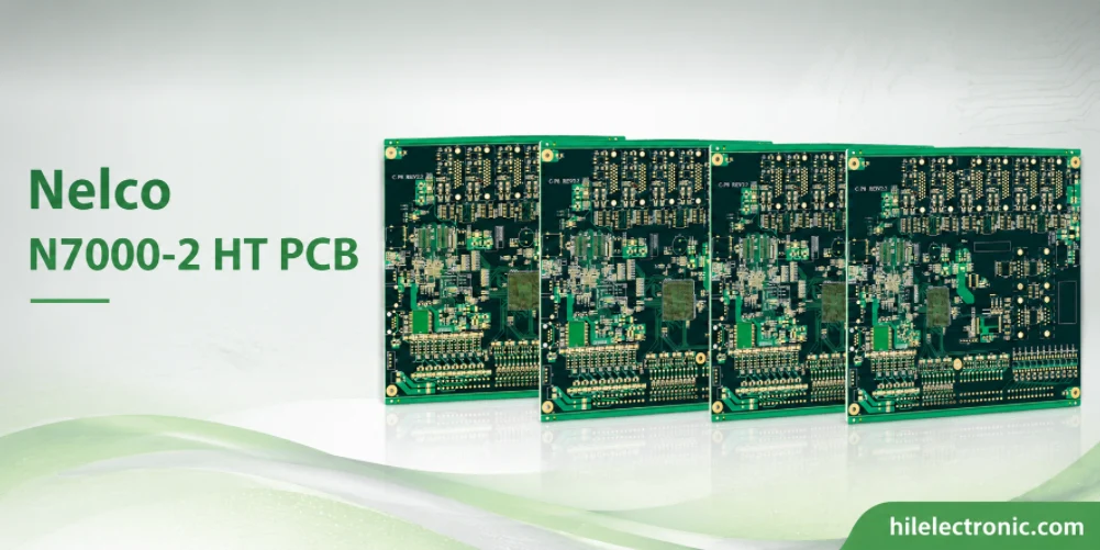
Two quotations that both say “Nelco N7000-2 HT” can describe different boards. Core and prepreg availability, resin content, copper profile, finished dielectric spacing, drill route, backdrill depth and test evidence determine whether the quoted construction matches the customer’s loss and reliability model.
Highleap approaches N7000-2 HT as a controlled multilayer build rather than a premium label. The exact current data sheet and available constructions should be confirmed with the material supply chain at quotation. Where availability requires an alternative, the proposed change must be documented, modelled where necessary and approved before production.
Is Nelco N7000-2 HT the Right Material for Your PCB?
N7000-2 HT is most relevant when the board needs a combination of lower transmission loss, high-temperature capability and robust multilayer processing. Typical opportunities include network equipment, server and storage hardware, test systems, aerospace or industrial electronics, and high-layer control platforms with long routed channels. It may also appear in hybrid material strategies where only selected signal layers require lower loss. The material decision should therefore follow the actual channel and construction, not a broad product label such as “100G board,” “server PCB” or “high-speed backplane.”
A short chip-to-chip route on a compact daughtercard can sometimes remain within margin on a more available high-Tg material. Conversely, a moderate lane rate can justify N7000-2 HT when the route is long, the board contains several connectors, the vias have meaningful residual stubs, or the finished board is thick enough to increase fabrication risk. This is why Highleap reviews the complete loss and reliability picture rather than comparing only a single dissipation-factor value.
| Project condition | What it means for selection | Information needed before release |
|---|---|---|
| Short on-board routes with one transition | N7000-2 HT may provide margin, but a lower-cost construction may also be sufficient. | Longest route, lane rate, receiver margin and permitted alternatives. |
| Long line card or backplane paths | Distributed dielectric and conductor loss become more important. | Insertion-loss target, connector models, copper profile and layer assignment. |
| High-layer or thick multilayer PCB | Registration, resin filling, drilling and plated-hole reliability must be considered with signal performance. | Layer count, finished thickness, drill sizes, copper distribution and thermal history. |
| Multiple reflow cycles or field thermal cycling | Material properties help, but hole geometry and manufacturing controls remain decisive. | Assembly profile, reflow count, rework expectation and reliability class. |
| Customer-controlled approved material list | No substitution should be made merely because another laminate appears electrically similar. | Exact grade, construction, certificate requirements and approval process. |
For buyers comparing several families, the most efficient starting point is a structured high-speed PCB material selection review. That comparison should use the same test method, frequency, resin content and copper condition. Published typical values from different data sheets are not automatically interchangeable, and they are not finished-board guarantees.
When is a material upgrade likely to create real value?
The upgrade creates value when dielectric loss represents a meaningful part of the channel and when the fabricator can preserve the assumed construction in production. If the channel is dominated by a poor connector launch, an open via stub, an oversized antipad, a reference-plane split or an uncontrolled return path, moving to a lower-loss laminate may not recover enough margin. The topology should be corrected first. If the board is dominated by through-hole reliability, the design team should also examine aspect ratio, finished hole size, minimum barrel copper and assembly exposure rather than relying on the material name as a universal solution.
When should another material be considered?
A more economical high-Tg system can be appropriate for short channels and mainstream multilayers. A still lower-loss family may be required for a long next-generation backplane after avoidable losses have been removed. A dedicated RF laminate may be more appropriate for antennas or microwave structures. Supply continuity can also determine the practical choice: if the exact N7000-2 HT core or prepreg construction has an unsuitable lead time, Highleap can present a manufacturable alternative for written customer approval, but it should not be substituted silently.
From Channel Requirements to a Manufacturable N7000-2 HT Stackup
The stackup is the bridge between simulation and factory production. A useful release identifies the exact laminate family, matching prepreg, target dielectric thicknesses, copper weights and copper profile. It also tells the fabricator which dimensions are electrical constraints and which are only preliminary modelling values. Without that distinction, a board shop may meet overall thickness while moving dielectric spacing in a way that changes impedance or channel loss.
Highleap normally begins with the finished board requirements and works backward through press constructions that are available in the required region and quantity. For a custom N7000-2 HT multilayer PCB, this review covers pressed prepreg thickness, resin demand around copper, glass styles, core availability, copper treatment, sequential lamination if any, drilling depth, backdrill access and panel utilisation. The proposed build is then returned for customer approval before production data are frozen.
Which dielectric values belong in the field solver?
Use construction-specific design values for the actual core or prepreg, not one marketing number copied from a comparison chart. Resin content, glass reinforcement, frequency, moisture, copper profile and test method influence the effective result. The impedance model should therefore be tied to a specific production construction. Highleap can calculate manufacturable trace dimensions from the approved stackup, but the system owner remains responsible for the channel model and protocol compliance.
How should copper be specified?
Copper is both an electrical and manufacturing variable. Low-profile copper can reduce conductor loss, especially as the operating spectrum moves upward, but it must be sourced in the required thickness and construction. Inner-layer treatment also affects the final surface seen by the signal. A drawing that says only “one ounce copper” does not fully define the finished trace: base foil, plating, etch compensation and surface treatment all influence geometry. For this reason, the quotation should identify whether the copper profile is mandatory, preferred or open to engineering proposal.
Where the signal-integrity margin is tight, the project can also specify the permitted insertion-loss test method or coupon. Where impedance is the primary control, use a clearly defined high-speed PCB impedance-control table with layer, geometry, reference planes and tolerance. Avoid ambiguous notes such as “all differential pairs 100 ohms” when several layer constructions are present.
Via architecture should be selected before the material is blamed
A high-layer board may require through vias, blind vias, buried vias, backdrilling or a combination. The correct choice depends on BGA escape, layer transitions, finished thickness, drill diameter and residual stub allowance. Backdrilling is useful only when the remaining stub, registration tolerance and drill access are controlled. It does not automatically improve every channel. Review the actual back-drilling construction and residual-stub requirement before the drill table is released.
What Makes a High-Layer N7000-2 HT Board Difficult to Manufacture?
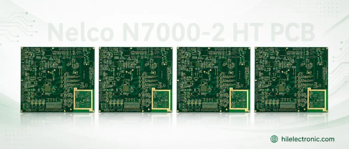
The material can support demanding boards, but production risk is still driven by geometry. High layer count increases the number of registration interfaces. Thick finished boards increase hole-wall strain and make desmear and plating more difficult. Dense copper creates resin-demand differences and can distort flow. Large panels magnify artwork compensation and warpage. These interactions explain why a quotation for a high-layer N7000-2 HT PCB should not be based only on square area and layer count.
During CAM review, Highleap checks annular rings, drill-to-copper spacing, antipads, backdrill clearances, copper balance, resin fill around plane clearances, rout tolerances, impedance coupons and assembly panel requirements. Where a design is too aggressive for stable yield, the engineering response should identify the specific conflict and propose a controlled change—not simply reject the project or promise that the factory can “try.”
Lamination and registration
Press cycles must provide complete cure and adequate resin flow without creating excessive thickness variation. High-copper inner layers, large plane openings and uneven copper density can produce local resin starvation or thickness imbalance. Registration targets must account for material movement, artwork scaling and drill wander. For large or very high-layer products, a trial panel can be more valuable than a nominally faster full production launch because it provides data for scaling and press compensation.
Drilling, desmear and plated-hole reliability
Mechanical drilling generates heat and smear; tool condition, hit count and feed parameters must match the construction. Desmear must clean the hole wall without damaging resin-to-glass integrity. Copper plating must achieve the drawing minimum throughout the barrel, including high-aspect-ratio holes. The laminate reduces risk only when these operations are controlled. Buyers with demanding thermal-cycling requirements should define the required coupon or qualification method rather than asking for a vague “high-reliability PCB.”
For projects where layer count and hole survival dominate the decision, the broader high-layer-count PCB material and reliability discussion can help separate material risk from geometry risk.
Assembly affects the bare-board decision
The bare board may later see double-sided SMT reflow, selective soldering, press-fit insertion, manual repair or repeated qualification cycles. Highleap therefore asks about the assembly process before finalising some stackups. If turnkey PCBA is required, stencil design, component moisture control, BGA profiles, support fixtures and inspection are planned with the PCB. This is more reliable than treating fabrication and assembly as unrelated orders.
How Highleap Reviews and Quotes an N7000-2 HT PCB Project
A fast response begins with complete data. Highleap can quote prototypes, low-volume builds and scheduled production, but special-material lead time must be confirmed before a quick-turn promise is made. The most useful package includes fabrication files, drawing, stackup, drill files, impedance requirements, quantities, panel or delivery format, assembly BOM and pick-and-place data where PCBA is required.
- Gerber, ODB++ or IPC-2581 fabrication data and a revision-controlled drawing;
- exact N7000-2 HT construction or permission to propose a build for approval;
- finished thickness, copper, surface finish, solder mask and dimensional tolerances;
- impedance table, critical channel layers, loss or coupon requirements;
- drill chart, via type, backdrill depths and residual-stub target;
- prototype and production quantities, target delivery and packaging method;
- BOM, centroid, assembly drawing, test instructions and programming files for turnkey PCBA.
After technical review, the quotation can state material availability, tooling or test charges, production lead time, assembly scope and shipping terms. Payment methods and currency are confirmed according to the order value and customer account. Prototype orders can usually travel by international express; larger production shipments can use courier, air freight or another agreed route. Packaging is selected to protect finished boards and assembled products during export handling.
Support continues after shipment. If a fabrication or assembly concern is reported, the lot record, inspection data and approved files can be reviewed by the engineering team. Corrective action depends on evidence from both sides, but traceable project records make the investigation faster and more useful than a generic warranty statement.
To request pricing, use a complete PCB fabrication and assembly quotation package. Highleap will identify missing engineering data before the order is released rather than allowing an ambiguous material or stackup note to become a production defect.
How a purchasing team can compare two N7000-2 HT quotations
Two prices are comparable only when they describe the same construction and evidence. Check whether both suppliers quoted the exact laminate and matching prepreg, the same copper profile, the same backdrill requirement, the same impedance tolerance and the same inspection package. One quotation may appear lower because it assumes a different core thickness, standard copper, no loss coupon or a broader material-substitution clause. Ask each supplier to return a proposed stackup and identify every assumption before selecting the source.
Lead time should also be separated into material procurement, PCB fabrication and assembly. A supplier may advertise fast PCB production while the required core or prepreg is not in stock. Highleap confirms material availability before promising the schedule. Where the customer has forecast demand, material reservation or a repeat-order construction can reduce future lead-time risk.
Repeat orders need controlled change management
A high-speed board that passes prototype validation can drift if a later order uses another glass style, foil profile, pressed thickness or CAM compensation. The purchase order should reference the approved stackup and artwork revision. Highleap records the released construction and submits material or process changes for approval when they can influence electrical or reliability performance.
For long-term programmes, the customer can define an approved-equivalent procedure. A proposed alternative should include manufacturer, grade, construction, relevant design data, copper and a revised impedance calculation. Depending on risk, the change may require a small qualification lot rather than full system requalification. This approach protects supply continuity without treating every laminate with a similar marketing category as identical.
PCB assembly can expose bare-board weaknesses
Large server and communication boards may carry heavy connectors, large BGAs, press-fit components and heat sinks. The assembly panel and fixture should support the board during reflow. Press-fit insertion forces should be considered around plated holes and local copper. If the project uses selective soldering after SMT, the extra thermal event belongs in the reliability plan.
When Highleap provides turnkey assembly, the board and assembly engineers share the stackup, panel, component and test information. This allows solder paste, reflow support, connector insertion, X-ray inspection and functional test to be planned before the bare board is completed. Customers using another assembler should still provide the expected thermal history so the fabrication quotation reflects the real service condition.
What “quality assurance” should mean for this project
Quality assurance should be a short list of controls tied to failure risk. For an N7000-2 HT backplane it may mean material traceability, impedance and insertion-loss coupons, residual-stub verification and connector-hole dimensional control. For a thick industrial controller it may mean hole-wall copper, thermal stress and bow/twist. A standard certificate stating that the board passed inspection does not replace project-specific acceptance criteria.
Highleap can agree on record retention and reporting before the order. This helps professional buyers avoid unnecessary documents while ensuring that the evidence needed for customer approval, field investigation or regulatory files is available. The same principle applies to after-sales support: a reported failure is investigated against lot, stackup, process and assembly data rather than answered with a generic statement.
Material note: properties and availability must be confirmed from the latest controlled Nelco data and the exact core/prepreg construction quoted for the project. Typical data are not finished-board guarantees.

Recommended Posts

Taconic RF-35 PCB Manufacturing Service — Prototype Through Volume Production
Figure 1. Taconic RF-35 PCBTaconic RF-35 is the workhorse...

Isola Astra MT77 PCB Manufacturing
Figure 1. Isola Astra MT77 PCB ManufacturingIsola Astra...

Custom Rogers RO4835 PCB Fabrication & Assembly Services
Figure 1. Rogers RO4835 PCBRogers RO4835 PCB is a...

Nelco N4000-13 PCB Material and Manufacturing Guide | Highleap Electronics
Figure 1. Nelco N4000-13 PCBNelco N4000-13 PCB is a...
How to get a quote for PCBs
Let’s run DFM/DFA analysis for you and get back to you with a report. You can upload your files securely through our website. We require the following information in order to give you a quote:
-
- Gerber, ODB++, or .pcb, spec.
- BOM list if you require assembly
- Quantity
- Turn time
For PCBA services, please provide your BOM (Bill of Materials) and any specific assembly instructions. We also offer DFM/DFA analysis to optimize your designs for manufacturability and assembly, ensuring a smooth production process.