
High Layer Count PCB Materials for Multilayer Boards
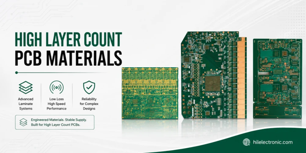
A high-layer-count PCB — 18, 24, 32 layers or more — is one of the most demanding products a fabricator builds, and the material it is built from is central to whether it succeeds. Each added layer multiplies the number of material interfaces that must bond cleanly, the registration tolerances that must hold across the stack, and the quantity of laminate and prepreg the board consumes. In 2026, high-layer-count boards also feel the material shortage most acutely, because they tend to require the scarcest grades in the largest quantities. This guide covers the material requirements, the core and prepreg selection, the yield and warpage challenges, and the supply realities.
Material Requirements for High Layer Count Designs
High-layer-count designs impose material requirements that low-layer boards do not. Dimensional stability is paramount: the material must hold its dimensions through multiple lamination cycles so that features on inner layers register accurately to one another and to the drilled holes. Z-axis CTE must be controlled, because the more layers and the thicker the board, the more total z-axis expansion occurs through thermal cycling, stressing plated through-holes. Consistent dielectric thickness and Dk across the panel are essential for impedance control on the many signal layers. And the resin system must bond reliably layer-to-layer without voids or resin starvation.
For high-rate high-layer-count boards — AI servers, high-speed switches — these requirements combine with a low-loss requirement, pushing the design toward mid-loss or low-loss grades on the signal layers. This is why high-layer-count and high-performance material requirements so often overlap. The application context is in AI server PCB materials and the design background in our multilayer PCB design guide.
Core and Prepreg Selection
A multilayer board alternates two material forms: cores (fully cured laminate with copper on both sides, carrying the inner signal and plane layers) and prepreg (B-stage resin-impregnated glass cloth that bonds the cores together during lamination and flows to fill between features). Selecting both correctly is essential. The core sets the inner-layer dielectric thickness and the impedance of the signal layers it carries; the prepreg sets the bond-layer thickness and must have the right resin content to flow and fill without starving or creating voids.
For high-layer-count boards the prepreg choice is particularly consequential because there are many bond layers, and each one is an opportunity for a void or a thickness error that affects impedance. Resin content and flow characteristics must be matched to the copper feature density on the adjacent layers — high-copper inner layers need prepreg with enough resin to fill the spaces between features. The core and prepreg should also share a compatible material system to bond reliably. The fundamentals are in our dedicated prepreg material for multilayer PCB guide and the PCB laminate construction overview.
Lamination Yield Considerations
Lamination yield falls as layer count rises, because each lamination cycle and each material interface adds a chance of a defect — a void, delamination, resin starvation, or a registration error — and the defects compound across the stack. High-layer-count boards often require sequential lamination (building up sub-assemblies in multiple press cycles), which multiplies the thermal and mechanical stress on the material and the number of registration steps that must hold.
Material choices directly affect this yield. A resin system with a well-characterized lamination profile, prepreg with appropriate flow for the feature density, and a balanced stack-up all raise first-pass yield. Conversely, a poorly matched prepreg or an unbalanced stack-up depresses yield, and on an expensive high-layer-count board a yield loss is costly — both in scrapped material (which is scarce and expensive in 2026) and in the lost material allocation that produced it. Reducing premium-CCL consumption and removing unnecessary lamination cycles through smart stack-up design therefore improves both cost and yield. The sequential-lamination background is in sequential lamination in HDI PCB.
Managing Warpage and Registration
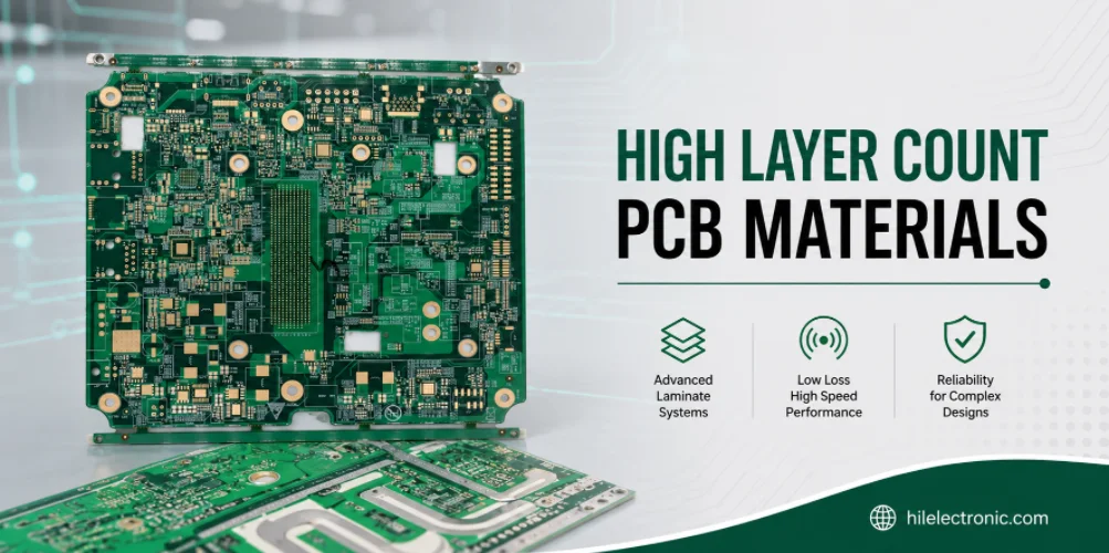
Warpage and registration are the two mechanical failure modes that high layer count makes worse, and both are partly material-driven. Warpage results from asymmetry — unbalanced copper distribution, asymmetric stack-ups, or mismatched material expansion — that causes the board to bow as it cools from lamination. The defenses are a symmetric stack-up (balancing copper and dielectric about the centerline), matched materials through the stack, and controlled lamination cooling. Warpage matters because a bowed board causes assembly problems: poor solder-paste registration and component-placement errors.
Registration — the accurate alignment of inner-layer features to one another and to the drilled holes — degrades as more layers stack because each layer adds dimensional movement during lamination. Materials with high dimensional stability and low movement under lamination heat hold registration better, which is why dimensional stability is a core high-layer-count material requirement. Tight registration is also what allows smaller annular rings and finer features on high-density boards. The design discipline is covered in our HDI stack-up design guide.
Material Lead Time Challenges
High-layer-count boards face the toughest material lead-time picture for two reasons. First, they often require the more constrained grades — high-layer-count high-performance boards use mid-loss to low-loss laminate, which runs 14–18 weeks for M6/M7 and 20+ weeks (allocation-only) for M8/M9. Second, they consume far more material per board than low-layer designs, so the allocation requirement is larger and harder to fill from a constrained supply.
The high-layer-count segment is also growing fast — high-layer-count multilayer boards (18+ layers) are among the fastest-growing PCB categories, driven by AI servers and high-speed networking — which adds demand pressure on exactly the grades that are most constrained. The practical response is the same as for other constrained boards: forecast early, qualify a second grade, plan material commitments 16–20 weeks ahead for premium grades, and use hybrid stack-ups where the design permits to limit the quantity of the scarcest grade. The lead-time mechanics are in our PCB laminate lead time guide and the supply context in the PCB material shortage Hub.
Manufacturer Stack-Up Review Process
For a high-layer-count board, the manufacturer’s stack-up review is the decisive quality and cost step. It confirms several things at once: that the impedance on every controlled-impedance layer is calculated with the actual laminate Dk and meets tolerance; that the stack-up is symmetric for warpage control; that the core and prepreg selection bonds reliably and fills the feature density; that the lamination plan (including any sequential lamination) is sound; and that the specified material grade is available — or has a qualified equivalent — given current allocation.
Because high-layer-count boards are expensive and the material is scarce, catching a stack-up, impedance, or availability problem before fabrication is far cheaper than discovering it in a failed lamination or an out-of-tolerance board. Highleap Electronics provides confirmed stack-up calculations using measured laminate Dk values and a pre-fabrication review covering impedance, symmetry, core/prepreg bonding, and material availability for high-layer-count designs.
Get a High-Layer-Count PCB Stack-Up Review
Highleap Electronics fabricates high-layer-count multilayer boards across these requirements. See our multilayer PCB, 16-layer PCB, and 28-layer PCB design capabilities, along with the 12-layer PCB reference.
High Layer Count PCB Materials FAQs
What material properties matter most for high-layer-count boards->
Dimensional stability (to hold registration through multiple lamination cycles), controlled z-axis CTE (for through-hole reliability), consistent dielectric thickness and Dk (for impedance control), and a resin system that bonds reliably without voids or starvation.
What is the difference between core and prepreg->
A core is fully cured laminate with copper on both sides, carrying inner signal and plane layers. Prepreg is B-stage resin-impregnated glass cloth that bonds the cores together during lamination and flows to fill between copper features. Both must be selected correctly for impedance and reliable bonding.
Why does lamination yield fall as layer count rises->
Each lamination cycle and material interface adds a chance of a void, delamination, resin starvation, or registration error, and these compound across the stack. High-layer-count boards often need sequential lamination, multiplying the stress and registration steps. Well-matched materials and balanced stack-ups raise yield.
How is warpage controlled on high-layer-count boards->
With a symmetric stack-up that balances copper and dielectric about the centerline, matched materials through the stack, and controlled lamination cooling. Warpage matters because a bowed board causes solder-paste registration and component-placement problems at assembly.
Why do high-layer-count boards face the worst material lead times->
Because they often require the more constrained grades (14-18 weeks for M6/M7, 20+ weeks allocation-only for M8/M9) and consume far more material per board, making the allocation requirement larger and harder to fill. Forecasting early and qualifying a second grade are essential.

Recommended Posts

Taconic RF 35 vs RO4350B PCB
Table of contentsRF-35 vs RO4350B Procurement and...

TMM4 Filter PCB Manufacturing
TMM4 filter PCB manufacturing is controlled by the...

TMM6 PCB Fabrication
TMM6 fabrication is the process-control page for a mid-Dk...

TMM3 PCB Manufacturing for RF Modules
TMM3 PCB manufacturing is most useful where the RF module...
How to get a quote for PCBs
Let’s run DFM/DFA analysis for you and get back to you with a report. You can upload your files securely through our website. We require the following information in order to give you a quote:
-
- Gerber, ODB++, or .pcb, spec.
- BOM list if you require assembly
- Quantity
- Turn time
For PCBA services, please provide your BOM (Bill of Materials) and any specific assembly instructions. We also offer DFM/DFA analysis to optimize your designs for manufacturability and assembly, ensuring a smooth production process.