
The Practical Guide to Multilayer PCB Design

In modern electronics, multilayer PCBs are essential for creating high-density, compact, and reliable circuits. These boards feature multiple layers of conductive material, typically interconnected by vias, to allow complex circuitry within a small footprint. Whether you are an electronics manufacturer looking to fabricate multilayer PCBs or an experienced designer trying to optimize your designs for manufacturability, understanding the core principles of multilayer PCB design is critical to the success of your products.
This guide will cover the essential aspects of multilayer PCB design, providing clear design rules, relevant formulas, material selection criteria, and simulation techniques to help you achieve high-performance PCBs that meet both functional and manufacturability requirements. Highleap Electronic offers the expertise to help you design parts, manage layer structures, and efficiently route complex multilayer PCB designs.
1. Key Considerations for Multilayer PCB Design
1.1 Material Selection: Balancing Performance and Cost
Choosing the right materials for multilayer PCBs is one of the most critical decisions you’ll make during the design process. The material impacts performance, durability, manufacturability, and cost. Key factors to consider include dielectric constant, thermal stability, and signal loss.
- FR-4: The most commonly used base material for standard PCBs, offering a good balance between performance and cost. It’s suitable for most applications where high-speed signal integrity is not the primary concern.
- High-Frequency Materials: For designs requiring high-speed or RF circuits, materials like Rogers 4350B or Teflon are preferred for their lower signal loss and higher dielectric constant stability over a wide temperature range.
- Thermal Management: For power-heavy applications, Thermal Management Materials (e.g., Aluminum Nitride (AlN)) are crucial in reducing thermal issues and preventing overheating.
1.2 Layer Stack-Up Planning
The layer stack-up is the arrangement of signal, power, and ground layers in the PCB. A well-planned stack-up ensures signal integrity and thermal management, and also reduces manufacturing complexity. Here’s a breakdown of critical design elements for planning your multilayer stack-up:
- Symmetric Stack-up: In most cases, it’s recommended to keep the stack-up symmetric (i.e., the same number of layers above and below the center). This minimizes warping during the manufacturing process.
- Signal Layers: These are the layers where active circuits are routed. Signal layers should be placed between ground and power planes to improve signal integrity by minimizing the distance between signal traces and the reference planes.
- Power and Ground Planes: At least one power plane and one ground plane are typically required for high-speed and high-density designs to provide clean, low-impedance paths for the signals.
For example, a typical 6-layer PCB stack-up might look like:
- Layer 1: Signal (Top)
- Layer 2: Ground Plane
- Layer 3: Power Plane
- Layer 4: Signal
- Layer 5: Ground Plane
- Layer 6: Signal (Bottom)

2. Signal and Power Integrity in Multilayer PCBs
Signal and power integrity are two of the most crucial factors in ensuring the reliable operation of high-speed electronic circuits. In multilayer PCB designs, managing signal integrity and power integrity becomes more complex due to the increased number of layers and the interactions between them. Proper design, analysis, and implementation of strategies such as impedance control, crosstalk mitigation, and power distribution are essential for achieving high-performance and low-noise designs.
2.1 Controlling Impedance and Crosstalk
In high-speed PCB designs, maintaining proper impedance control is essential to avoid signal degradation and reflections that can cause data errors. Impedance mismatch occurs when the resistance seen by the signal in its path is inconsistent, leading to signal reflections and potential data loss. The goal is to ensure that the signals are transmitted with minimal attenuation, distortion, and reflection.
Impedance Control
Impedance control refers to the management of the characteristic impedance of signal traces on the PCB. Impedance should be kept consistent along the trace length, especially for high-speed signals, to ensure signal integrity. The three most common types of impedance used in PCB design are single-ended impedance, differential impedance, and controlled-impedance routing.
Key Considerations:
- Trace Width and Spacing: The width of the trace, its distance from the ground plane, and the type of material used in the PCB determine the impedance of a trace. For example, to achieve a differential impedance of 100Ω (common in high-speed designs like USB or HDMI), the trace width and the spacing between the traces in a differential pair must be calculated with precision.
- Transmission Line Effects: When routing traces at high speeds, they act as transmission lines, and the impedance must be consistent to avoid reflections. The most common methods for controlling impedance include microstrip (trace on the surface above a reference plane) and stripline (trace sandwiched between two reference planes).
Formula for Impedance Calculation: To calculate the characteristic impedance of a PCB trace, the following formula can be used for a microstrip line:
This formula helps determine the optimal trace width based on the desired impedance for the signal type.
Differential Pair Routing
For high-speed differential signals (e.g., USB, HDMI, PCIe), it is essential to route differential pairs with a consistent impedance of around 100Ω. Differential signals consist of two complementary signals, and the difference between the two is the information carried. These pairs must be routed in parallel, ensuring the signal integrity is preserved throughout the trace length.
Key Guidelines:
- Trace Width and Spacing: The width of each trace in a differential pair and the spacing between them should be controlled to maintain the desired impedance. Typically, this requires precise measurements and simulation using software tools such as Altium Designer or Ansys HFSS.
- Matching Length: The length of the traces in a differential pair must be matched as closely as possible to avoid skew, where one signal arrives earlier than the other, causing timing errors.
Crosstalk Minimization
Crosstalk refers to the unwanted coupling between adjacent traces, resulting in signal interference and degradation. In multilayer PCB designs, crosstalk is an issue that becomes more prominent as the number of layers increases. Perpendicular routing of adjacent signal traces is one of the most effective methods to minimize crosstalk.
Key Strategies:
- Layer Stack-Up Design: Ensure that signal layers are placed perpendicular to adjacent layers to minimize the opportunity for electromagnetic coupling between signals.
- Spacing Between Signals: Increase the spacing between high-speed signal traces to reduce the chance of crosstalk, particularly in high-frequency applications where signals can easily induce noise in nearby traces.
- Ground Planes as Shields: Use ground planes between signal layers to act as shields, effectively reducing the risk of crosstalk and improving signal integrity.
2.2 Power Integrity and Grounding
Power integrity refers to the ability of the power distribution network (PDN) to provide clean, stable power to all components across the PCB. Grounding is equally crucial, as it provides the reference point for signals and minimizes the risk of ground noise or fluctuations, which can cause issues like ground bounce or voltage dips.
Power Distribution Network (PDN)
The PDN is responsible for delivering power to all components on the PCB, and its design directly impacts the board’s performance. A stable PDN ensures that the components receive the correct voltage and prevents voltage drops, which could otherwise lead to instability or malfunction.
Key Components:
- Power Planes: A dedicated power plane provides a uniform distribution of voltage across the PCB. The power plane should be wide and continuous, ensuring that the voltage supplied to the components is consistent.
- Decoupling Capacitors: These are essential for maintaining power integrity. Capacitors should be placed as close as possible to high-frequency components to filter out high-frequency noise and smooth out voltage fluctuations.
- Via Stitching: Via stitching is used to connect power and ground planes across multiple layers to reduce inductive effects and improve the power distribution network. It also helps reduce the impedance between planes.
Grounding Techniques
A continuous ground plane is fundamental in ensuring signal integrity and preventing issues like ground bounce. Ground bounce occurs when the voltage potential of the ground plane fluctuates due to high current flows or switching signals.
Guidelines:
- Continuous Ground Plane: Keep the ground plane continuous with as few breaks as possible. This minimizes impedance and reduces noise in the system.
- Via Stitching for Grounding: Use via stitching to interconnect the ground plane between layers, ensuring that the ground connection remains solid throughout the design. This technique also helps prevent ground loops, where multiple paths to ground can lead to variable ground potentials.
- Avoid Split Ground Planes: Split ground planes should be avoided in high-speed designs, as they can cause fluctuations in the ground potential and introduce noise. Use a solid ground plane to ensure a stable reference point.
Reducing Power Noise
Power noise can degrade the performance of high-speed circuits, particularly in sensitive analog components. To mitigate power noise:
- Use multiple ground planes to isolate noisy signals from sensitive ones.
- Use dedicated planes for power and ground to avoid interference from high-speed signals.
Maintaining signal integrity and power integrity is vital for ensuring the proper operation of high-speed and high-performance systems on multilayer PCBs. By controlling impedance, minimizing crosstalk, and implementing effective grounding and power distribution strategies, PCB designers can create reliable, noise-free designs that meet the demands of modern electronics. These practices are essential for manufacturers looking to produce high-quality PCBs that will perform under demanding conditions, especially in high-frequency and high-power applications.

3. Advanced Design Considerations
When designing multilayer PCBs, advanced considerations such as via selection and thermal management play a critical role in ensuring optimal performance, manufacturability, and reliability. These factors become especially important as the complexity of the design increases, requiring careful planning and the use of advanced techniques to address challenges such as signal integrity, heat dissipation, and space constraints. In this section, we’ll explore the various via types, their optimal placement strategies, and best practices for managing heat effectively in multilayer PCB designs.
3.1 Via Types and Placement
Vias are essential components in multilayer PCB designs, allowing for electrical connections between different layers. Proper via selection and placement can have significant implications for both the performance and manufacturability of the PCB. The choice of via type not only impacts the signal integrity but also affects thermal dissipation, density, and cost.
1. Through-Hole Vias
Through-hole vias are the most commonly used via type and run from the top layer to the bottom layer, connecting all internal layers of the PCB. These vias are typically larger in diameter, making them easier to fabricate but less suitable for high-density interconnections (HDI).
- Advantages:
- Cost-effective for low-to-mid complexity designs.
- Simple to manufacture.
- Suitable for large components and high-current paths.
- Disadvantages:
- Take up valuable space, especially on high-density designs.
- Larger diameter can increase the current resistance.
2. Blind Vias
Blind vias connect the outer layers to one or more inner layers but do not extend through the entire PCB. They are often used to save space and improve signal integrity by preventing the interference that through-hole vias can cause.
- Advantages:
- Space-saving by eliminating the need for through-hole vias.
- Reduces signal degradation, particularly in high-frequency designs.
- Disadvantages:
- More expensive and harder to fabricate than through-hole vias.
- Require more careful layer planning to avoid errors in routing.
3. Buried Vias
Buried vias are used to connect two or more inner layers and are not visible on the outer layers of the PCB. These are typically used in high-density interconnect (HDI) designs, where maximizing the usable space on the outer layers is essential.
- Advantages:
- Maximizes outer layer space, allowing for more efficient routing.
- Enhances signal integrity by preventing signal interference from the outer layers.
- Disadvantages:
- The most difficult to manufacture and require more advanced PCB fabrication techniques.
- Higher cost due to the complexity of fabrication.
4. Micro Vias
Micro vias are typically used in HDI PCB designs, where space is at a premium and high-density interconnects are required. These vias are usually smaller than 0.2mm in diameter and are created using laser drilling technology.
- Advantages:
- Extremely space-efficient, ideal for high-density applications.
- Reduces board size and allows for more layers without increasing the footprint.
- Disadvantages:
- Expensive to manufacture due to the precision required.
- Not suitable for high-current or power applications because of their small size.
Via Placement Strategy
When placing vias in multilayer PCB designs, it’s important to ensure that the vias are positioned in such a way that they minimize signal integrity issues and manufacturing complexity:
- Via Density: Avoid overcrowding the PCB with vias, as too many vias can increase the overall impedance, reduce signal integrity, and complicate the manufacturing process.
- Via Placement: Place vias close to the components they are connecting to reduce trace length and minimize signal reflection. In high-speed designs, vias should be positioned to optimize impedance matching.
- Via Size: Always choose the smallest possible via size that can handle the required current and ensure proper electrical performance. Micro vias are ideal for high-density designs but should be avoided for power-critical paths.
Always work closely with your PCB manufacturer to determine the best via types and placement strategies based on the specific requirements of your design.
3.2 Thermal Management in Multilayer PCBs
In high-performance multilayer PCBs, especially those used in power-sensitive or high-speed applications, thermal management is essential. Without effective heat dissipation, components may overheat, leading to failure or reduced lifespan. Thermal vias, copper pours, and heat sinks are all critical to managing the heat generated by components, ensuring that the PCB remains functional and reliable over time.
Thermal Vias
Thermal vias are used to conduct heat from the heat-sensitive components to the PCB’s opposite side or to a dedicated heat sink. Thermal vias are generally larger than signal vias to accommodate higher thermal conductivity.
- Design Guidelines:
- Use multiple thermal vias beneath high-power components to improve heat conduction.
- For high-power components, place thermal vias as close as possible to the component’s heat source to increase heat dissipation efficiency.
- Key Consideration: Ensure that the via pitch (spacing between vias) is optimized to handle the thermal load. Too few vias can result in inadequate heat dissipation, while too many can lead to an increase in manufacturing complexity and cost.
Copper Pouring and Heat Sinks
Copper pouring is the process of filling unused areas of the PCB with copper to act as a heat sink. This copper pour helps to spread heat more effectively and prevent localized hotspots.
- Design Tips:
- Use large copper pours around the heat-generating components to act as thermal conductors and improve heat dissipation.
- Thermal vias should be connected to the copper pours to direct heat away from components and improve the cooling process.
In addition to copper pours, external heat sinks can be used to further increase the cooling capacity of the PCB. Heat sinks are typically attached to the PCB with thermal adhesive and are designed to dissipate heat away from the components.
Thermal Simulation
Before finalizing the design, performing thermal simulations is crucial to predict potential overheating areas and make necessary adjustments. Thermal analysis tools such as ANSYS Icepak or SolidWorks Flow Simulation can help identify areas that need additional thermal vias or copper pours.
PCB Layer Configuration for Thermal Management
Proper layer configuration plays an important role in thermal management. Having dedicated power and ground planes not only improves signal integrity but also helps in dissipating heat efficiently.
- Use of Ground Planes: Ground planes serve as an effective heat sink, improving heat dissipation across the PCB.
- Layer Symmetry: A symmetrical stack-up reduces the risk of warping due to thermal expansion, ensuring that the PCB remains stable under varying temperature conditions.
By integrating these thermal management strategies during the design phase, you can ensure the stability and longevity of your multilayer PCBs.
Advanced considerations such as via selection and thermal management are essential to achieving a well-functioning, reliable multilayer PCB. The choice of via types (through-hole, blind, buried, micro vias) must be carefully considered based on the complexity, density, and cost of the design. Meanwhile, effective thermal management ensures that heat-sensitive components remain within safe operating temperatures, preventing overheating and failure.
By applying the right strategies for via placement and incorporating proper thermal management techniques, you can significantly enhance the performance, manufacturability, and reliability of your multilayer PCB designs. Always ensure to collaborate with your PCB manufacturer to align on design constraints and to optimize the design for both functionality and production.

4. Design for Manufacturability (DFM) and Design for Assembly (DFA)
4.1 DFM and DFA Best Practices
Designing a PCB for manufacturability and assembly is key to reducing costs and ensuring the board is produced without errors. The following guidelines are essential for optimizing your design:
- Via Sizes: Ensure that vias meet the minimum size requirements specified by the manufacturer.
- Trace Width and Spacing: Use the manufacturer’s guidelines for trace widths and clearances to ensure proper fabrication.
- Component Placement: Arrange components so that they are easy to assemble. Avoid placing components too close to the edge of the board or too close to other components, which could complicate the assembly process.
4.2 Communication with Manufacturers
Collaboration with your PCB manufacturer is crucial. Discuss these aspects:
- Manufacturing capabilities: Maximum layer count, minimum trace width, via types, and tooling options.
- Lead times and cost considerations: More complex designs with high layer counts can increase both cost and lead time.
Conclusion
Multilayer PCB design is a complex process that requires careful consideration of various factors, including material selection, impedance control, signal integrity, and thermal management. Whether you are designing a high-speed communication circuit or a high-power application, understanding these key principles and applying them effectively will ensure that your designs are not only functional but also manufacturable.
As technology continues to advance, new materials, design techniques, and manufacturing methods will evolve. Staying up to date with these trends, and working closely with your manufacturer, will help you produce efficient, high-performance PCBs for the next generation of electronic devices.
Get a Free PCB & PCBA Quote

Recommended Posts

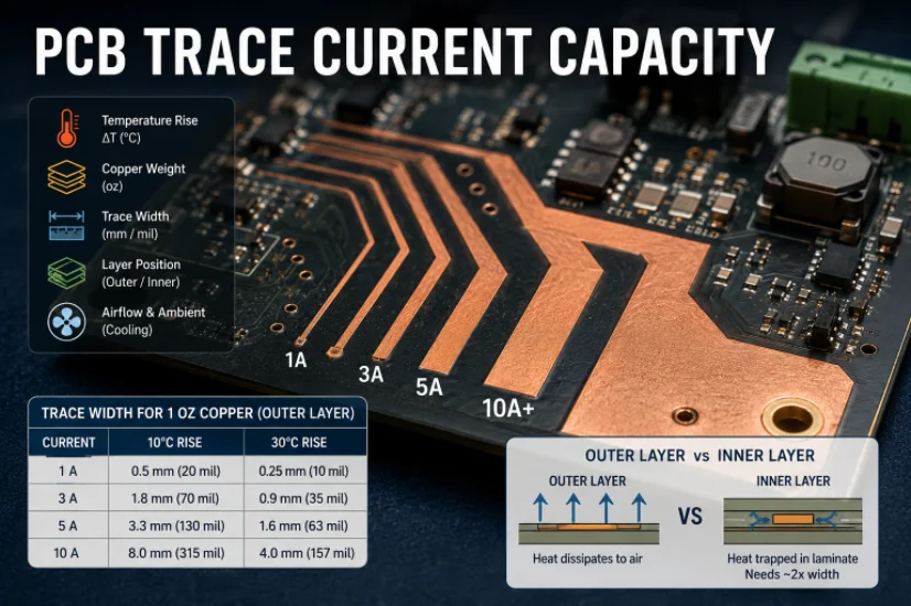
PCB Current Calculator: Sizing Trace Width and Vias with the IPC-2221 Formula
Figure 1. Pcb Current Calculator reference image for PCB...

Microphone PCB Design: How the Board Itself Shapes Your Audio Quality
Figure 1. Microphone Pcb reference image for PCB...
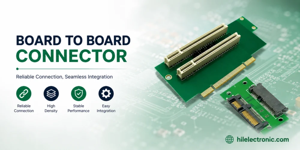
Board-to-Board Connector: Types, Specifications, and How to Select One
Figure 1. Board To Board Connector reference image for PCB...
PCB Trace Width Calculator: How to Size Traces for Current, Voltage Drop, and Impedance
Figure 1. A PCB trace width calculator is a starting point...
How to get a quote for PCBs
Let us run DFM/DFA analysis for you and get back to you with a report.
You can upload your files securely through our website.
We require the following information in order to give you a quote:
-
- Gerber, ODB++, or .pcb, spec.
- BOM list if you require assembly
- Quantity
- Turn time
In addition to PCB manufacturing, we offer a comprehensive range of electronic services, including PCB design, PCBA (Printed Circuit Board Assembly), and turnkey solutions. Whether you need help with prototyping, design verification, component sourcing, or mass production, we provide end-to-end support to ensure your project’s success. For PCBA services, please provide your BOM (Bill of Materials) and any specific assembly instructions. We also offer DFM/DFA analysis to optimize your designs for manufacturability and assembly, ensuring a smooth production process.