
Hybrid PCB Stackups for RF Circuit Design | Optimizing RF Performance and Cost

RF (Radio Frequency) circuit design is a specialized field within electrical engineering that combines electromagnetic theory, signal integrity, impedance matching, and high-frequency design principles. RF circuits play a vital role in modern technologies such as wireless communication, radar systems, broadcasting, and other advanced applications. In this article, we’ll explore the fundamentals of RF circuit design, the key components involved, essential design principles, and how RF design integrates with hybrid PCB technology for enhanced performance.
Introduction to RF Circuit Design
RF circuits operate at frequencies typically ranging from 3 kHz to 300 GHz, and their design differs significantly from that of low-frequency circuits due to the unique behavior of electromagnetic waves. These circuits involve a combination of passive components like resistors, capacitors, and inductors, as well as active components such as oscillators, amplifiers, and transceivers, which help shape and process high-frequency signals.
One of the core challenges in RF circuit design is understanding how signals propagate as electromagnetic waves and how materials and circuit layouts can influence these signals. Unlike low-frequency circuits, RF designs must accommodate the inherent characteristics of these waves, such as impedance matching, attenuation, and reflection, to ensure effective signal transfer.
Key Concepts in RF Circuit Design
- Passivity and Linearity: RF circuits can be either passive or active. Passive components, such as capacitors and inductors, do not amplify or generate power but influence the signal in terms of filtering or resonance. RF circuit behavior is usually linear, meaning that the relationship between input and output follows a straight line. Nonlinearity occurs when semiconductor devices such as diodes or transistors are added.
- Signal Propagation: RF circuits depend heavily on wave propagation principles, meaning the layout must account for transmission lines and the propagation of signals across different sections of the circuit. Proper impedance matching is crucial to prevent signal loss and reflections, which can degrade the signal quality.
- Electromagnetic Interference (EMI) and Shielding: RF circuits are particularly susceptible to electromagnetic interference, which can introduce noise into the system. To minimize this, shielding and isolation are critical design techniques, ensuring that signals remain clean and free from external disturbances.
- Impedance Matching: Achieving proper impedance matching between various elements of an RF circuit is vital for maximum power transfer and to avoid reflection, which can lead to inefficient operation. The design of transmission lines and components must consider the characteristic impedance of the circuit to achieve optimal signal flow.
Printed RF Circuits: Design and Implementation
In RF circuit design, printed circuit boards (PCBs) are commonly employed to construct the circuits. These boards utilize copper traces to form electrical connections, which are strategically laid out to manage signal flow and impedance. Unlike traditional low-frequency PCBs, RF circuit boards require meticulous planning of trace widths, layer stackups, and the selection of materials to preserve the integrity of high-frequency signals. Achieving precise control over signal behavior is critical in RF circuits to avoid signal degradation, interference, and impedance mismatch.
Key Components in Printed RF Circuits
- Transmission Lines
Transmission lines are one of the most crucial components in RF designs. They act as the pathway for RF signals, transmitting them between different parts of the circuit while maintaining the correct impedance. The design of transmission lines on a PCB is integral to the overall performance of the circuit, as improper impedance matching can lead to signal reflections, losses, and distortion. A typical design target is 50 ohms for most RF applications, ensuring that the signal is transmitted efficiently without any reflections. The choice of transmission line depends on the required frequency and application. Examples include microstrips, striplines, and coplanar waveguides. - Capacitors and Inductors
In RF circuits, capacitors and inductors play an essential role in controlling the frequency characteristics of the circuit. These components can be either discrete components or integrated directly into the PCB layout as printed elements. They are responsible for filtering unwanted signals, storing energy, and influencing the resonance of the circuit. Capacitors are often used for decoupling and filtering high-frequency noise, while inductors are employed in applications requiring inductive reactance, such as tuning filters or providing impedance matching. The precise layout of these components is critical to ensuring that the intended resonant frequencies are maintained. - Active Components
Active components, such as transistors, diodes, and integrated circuits (ICs), are often used in RF circuits to perform tasks such as amplification, oscillation, and signal modulation. These components can modify the amplitude, phase, or frequency of the RF signal. For instance, transistors are commonly used in amplifiers to boost signal strength, while oscillators generate stable RF signals for transmission. The integration of active components allows the RF circuit to perform more complex functions, such as frequency mixing, signal modulation, and processing, which are essential in systems like wireless communication, radar, and broadcasting.

Frequency Selection and Its Impact in RF Design
Frequency selection in RF circuit design is crucial for optimizing system performance. Different frequency bands (such as low, medium, and high frequencies) have varying requirements for PCB design, material selection, and component layout. Understanding how to select the appropriate frequency range for different applications (such as Wi-Fi, 5G, radar, etc.) and analyzing the impact of frequency choice on circuit performance, materials, and layout design is essential for RF engineers.
Low-Frequency RF vs. High-Frequency RF Design
Low-Frequency RF Design
Low-frequency RF (typically ranging from 3 kHz to 1 GHz) circuit design is simpler compared to high-frequency designs. At lower frequencies, signal loss is minimal, and signal attenuation is slower, meaning lower-frequency circuits require less stringent material selection. Materials such as FR4 are often sufficient for low-frequency designs. However, as the frequency increases, signal attenuation becomes more significant, requiring careful attention to signal integrity and circuit stability.
High-Frequency RF Design
High-frequency RF (1 GHz and above, especially in 5 GHz and millimeter-wave frequencies) design is more complex. As frequency increases, signal attenuation accelerates, and the characteristics of electromagnetic waves become more complex. High-frequency circuits demand more precise material selection and stricter layout regulations. High-frequency signals require accurate impedance matching, transmission line design, ground plane design, and electromagnetic interference (EMI) control. Materials like PTFE (polytetrafluoroethylene) and ceramic substrates are commonly used due to their lower loss and better electromagnetic characteristics.
Main Differences Summary
- Signal Attenuation: Low-frequency signals experience less attenuation, whereas high-frequency signals experience more, requiring higher-quality materials and design to reduce loss.
- Material Selection: FR4 is commonly used for low-frequency designs, while low-loss materials like PTFE and ceramic are preferred for high-frequency designs.
- Impedance Matching: High-frequency circuits require stricter impedance matching compared to low-frequency designs, where the requirements are more relaxed.
Challenges in High-Frequency Circuit Design: Optimizing Materials and Transmission Lines
1. Material Selection
The performance of high-frequency circuits is heavily influenced by the materials used. While standard FR4 works well for lower frequencies, it introduces excessive loss at high frequencies. High-frequency designs need materials that exhibit low loss, stable dielectric properties, and reliable performance at elevated frequencies. Commonly used materials for high-frequency RF circuits include:
- PTFE: Offers very low loss factors and stable dielectric properties, making it ideal for microwave and millimeter-wave circuits.
- Ceramic Substrates: Used in high-performance applications, such as radar systems, that require extremely high frequencies and precise electrical performance.
- High-Frequency FR4: An optimized version of FR4 for high-frequency applications, providing better performance but still having higher losses compared to PTFE.
2. Transmission Line Design
The design of transmission lines is crucial to ensuring efficient signal transmission at high frequencies. High-frequency signals require precise impedance control to avoid signal degradation, reflections, and attenuation. The commonly used transmission line types for high-frequency circuits include:
- Microstrip Lines: Used for surface-mount designs, these lines create stable transmission paths on the PCB surface.
- Stripline: Used for more complex circuits, especially in high-speed digital signal transmission.
- Coaxial Cables and Waveguides: Used for transmitting high-frequency signals over long distances, providing very low loss.
3. Impedance Matching and Reflection Control
Impedance matching is a key challenge in high-frequency circuit design. Mismatched impedance causes signal reflections, reducing signal strength and potentially introducing noise into the system. Ensuring precise impedance matching through the design of transmission lines is vital. Engineers use advanced design tools and formulas to ensure that each transmission line has the correct impedance to avoid reflection and signal loss.
4. Electromagnetic Interference (EMI) Control
As frequencies increase, the potential for electromagnetic interference (EMI) increases as well. High-frequency signals are more likely to radiate electromagnetic waves that can interfere with nearby circuits. Therefore, controlling EMI is critical in high-frequency designs, particularly in 5G, radar, and other high-performance applications. Solutions include using shielding materials, designing optimized ground planes, and using proper layout techniques to minimize the impact of EMI.
The Impact of Frequency Selection on Circuit Performance, Materials, and Layout Design
1. Signal Attenuation and Frequency Relationship
As frequency increases, the signal attenuation also increases. High-frequency signals experience more loss due to their shorter wavelength and greater interaction with the PCB and its components. This necessitates the use of low-loss materials and careful transmission line design to reduce the impact of attenuation on signal strength.
2. Layout and Layout Density
High-frequency circuits require much more precise layout design. At higher frequencies, the density and spacing between components have a significant impact on the quality of the signal. Designers must ensure that signal paths are kept as short as possible and that unnecessary crossings or signal path complexity are avoided. Layout flexibility is crucial, as high-frequency circuits need to balance performance with PCB space constraints.
3. Electromagnetic Compatibility (EMC)
As frequency increases, electromagnetic compatibility (EMC) becomes more critical. High-frequency signals can easily cause interference or radiation, impacting other nearby electronic systems. In high-frequency designs, especially in 5G, radar, and millimeter-wave applications, designers need to ensure that the PCB layout minimizes radiation and prevents noise coupling from digital or power circuits. Solutions include optimized circuit layout, shielding, and grounding techniques to comply with EMC standards.
For a more complete production review, use this article alongside DFM review and custom circuit board cost factors when checking stackup, assembly, or test requirements.
Design Considerations for Printed RF Circuits
When designing RF circuits on a PCB, there are several factors that must be taken into account to ensure the circuit operates as intended:
-
Trace Width and Impedance Control
The width of the traces used to create transmission lines is a critical factor in determining the impedance of the circuit. By adjusting the width of the traces and considering the thickness of the PCB and the dielectric constant of the material, designers can calculate the required width to maintain a specific impedance (commonly 50 ohms). This calculation ensures that the signal is transmitted efficiently and with minimal loss. -
Layer Stackup
The layer stackup of an RF PCB defines the arrangement of the different layers of the board, including the signal layers, ground planes, and power distribution. The stackup must be designed carefully to achieve the desired impedance for the transmission lines and to minimize parasitic effects like inductance and capacitance. For high-frequency applications, materials with low loss, such as PTFE-based laminates, are often used for the signal layers to reduce signal attenuation. -
Material Selection
The materials used in the PCB construction are crucial for high-frequency performance. Common materials for RF PCBs include FR4 for lower-frequency applications, and PTFE (Teflon) or ceramic-based laminates for high-frequency circuits. The choice of material influences factors such as signal loss, thermal conductivity, and the dielectric constant, all of which can affect the performance of the RF circuit. -
Signal Integrity
Maintaining signal integrity is paramount in RF circuit design. Signal degradation can occur due to noise, reflections, or interference, which can distort the transmitted signal and reduce the efficiency of the system. Shielding, proper grounding, and the use of low-loss materials are key techniques used to preserve signal quality. -
Minimizing Parasitic Effects
At high frequencies, parasitic inductance, capacitance, and resistance can become significant and affect the performance of the circuit. Careful layout design, such as minimizing the length of signal traces and avoiding unnecessary vias, can help reduce parasitic effects. Additionally, designers should ensure that the ground planes are continuous and free of interruptions to maintain proper signal return paths.
Hybrid PCB Stackups in RF Circuit Design
The performance of RF circuits is heavily influenced by the design of the PCB stackup. The stackup defines how the layers are arranged within the PCB and directly impacts the impedance characteristics, signal integrity, and overall functionality of the circuit. In RF design, stackup selection is critical and must be carefully tailored to the specific requirements of the frequency range, signal quality, and the materials used. A key innovation in RF circuit design is the development of hybrid PCB stackups, which use a combination of materials and configurations to optimize performance for both high-frequency RF and digital components.
The Importance of Hybrid PCB Stackups for RF Circuits
RF circuit boards operate at much higher frequencies than typical digital systems, making them more susceptible to signal degradation and interference. As a result, the PCB stackup must be carefully engineered to meet the unique needs of RF signals, including the requirement for low loss, controlled impedance, and minimized electromagnetic interference. The concept of hybrid PCB stackups addresses these challenges by strategically combining different materials and layer configurations to balance the performance demands of RF and digital systems.
Key Features of Hybrid PCB Stackups for RF Circuits
- RF Materials in Top Layers
In hybrid stackups, the upper layers of the PCB are typically composed of high-performance materials that are optimized for RF signal transmission. PTFE (polytetrafluoroethylene)-based laminates are often used in the top layers because of their low loss tangent, which ensures minimal signal attenuation at high frequencies. These materials are ideal for the creation of microstrip transmission lines, antennas, and other RF elements that require precise impedance control. By placing these materials in the top layers, the PCB design ensures that high-frequency signals are transmitted efficiently, maintaining the integrity of the RF signal. - Standard Materials for Internal Layers
The internal layers of a hybrid PCB stackup often use more conventional materials, such as FR4, which is cost-effective and commonly used in digital circuit designs. These layers typically carry digital signals, power distribution, and ground planes. While FR4 is not ideal for high-frequency applications due to its higher loss characteristics compared to PTFE, it is more than adequate for lower-frequency digital circuits and power routing. By using FR4 or similar materials in the internal layers, designers can balance the cost of manufacturing with the performance requirements of the RF components. This approach reduces the overall cost of the PCB while still optimizing the performance of the RF section on the surface layers. - Separation of RF and Digital Signals
One of the key benefits of a hybrid stackup is the ability to separate the RF and digital signal paths. RF signals are extremely sensitive to noise and interference, and integrating them with high-speed digital signals can lead to significant signal degradation. In a hybrid PCB, the RF components are typically isolated in their own layers, which helps prevent noise from digital circuits from contaminating the RF signals. Additionally, this separation can reduce the need for complex shielding, as the ground planes and signal layers can be optimized to ensure that the RF signals travel in a controlled and interference-free environment. - Impedance Control
Impedance control is crucial in RF circuit design, and the choice of materials and stackup configuration plays a key role in maintaining the desired impedance. In a hybrid PCB, the top layers that carry the RF traces are designed with precise impedance control in mind. Transmission lines, such as microstrips or stripline configurations, are used to guide RF signals while maintaining a constant impedance (usually 50 ohms). The internal layers, typically used for power and ground planes, help ensure that the impedance of the RF transmission lines is consistent and that signal integrity is preserved. - Thermal Management
RF circuits, especially those with active components, can generate significant heat. Hybrid PCBs, by separating RF and digital components, can also assist with thermal management. The use of high-performance materials in the upper layers ensures that the heat generated by RF components is effectively dissipated. Additionally, the use of internal layers for power distribution can help direct heat away from sensitive RF components, maintaining the overall stability and reliability of the circuit.
Benefits of Hybrid PCB Stackups for RF Design
- Improved RF Performance: By using materials optimized for high-frequency operation in the top layers, hybrid PCBs ensure that RF signals are transmitted with minimal loss, distortion, and noise.
- Cost Efficiency: Hybrid stackups combine the high-performance materials needed for RF circuits with more affordable materials for digital and power components. This cost-effective approach reduces overall PCB manufacturing costs without sacrificing performance.
- Noise Isolation: The separation of RF and digital components on different layers minimizes noise interference, improving the overall signal integrity and reducing the need for complex shielding techniques.
- Optimized Impedance Control: Hybrid stackups enable precise impedance control for RF transmission lines, ensuring that the circuit performs optimally at high frequencies.
Hybrid PCB stackups represent a significant advancement in RF circuit design, offering a balanced approach to optimizing both high-frequency performance and cost-efficiency. By using specialized materials in the top layers for RF signal transmission and standard materials in the internal layers for digital and power components, hybrid stackups provide the flexibility needed to create high-performance RF systems that also integrate seamlessly with digital circuitry.
This innovative approach allows engineers to meet the stringent requirements of modern RF designs while maintaining cost-effectiveness and simplifying the overall PCB manufacturing process. As the demand for RF circuits continues to grow, especially in fields like wireless communication, radar, and IoT, hybrid PCB stackups will play an essential role in advancing RF circuit design techniques.
Conclusion
RF circuit design is a specialized field that combines electromagnetic theory with electrical engineering principles. By optimizing signal propagation, impedance matching, and PCB layouts, engineers can develop efficient and high-performance RF systems for a wide range of applications, from cutting-edge communication networks to advanced radar technologies.
The integration of hybrid PCBs, which combine various materials and layer configurations, is a game-changer in RF design. This innovative approach allows engineers to build systems that are not only cost-effective but also tailored for maximum performance. At Highleap Electronic, we specialize in PCB manufacturing and assembly, offering expert solutions for hybrid PCBs that meet your specific design needs. As the demand for wireless communication and high-frequency technologies grows, RF circuit design and PCB hybridization will be at the forefront of transforming modern electronics. Partner with us to stay ahead in the rapidly evolving world of high-tech applications, with reliable and performance-driven PCBs built to the highest industry standards.
Get a Free PCB & PCBA Quote

Recommended Posts

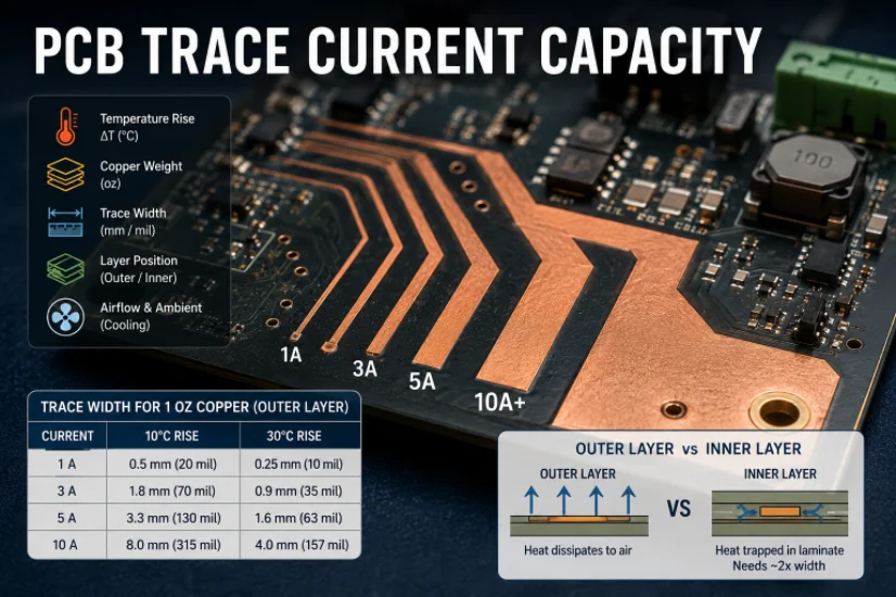
PCB Current Calculator: Sizing Trace Width and Vias with the IPC-2221 Formula
Figure 1. Pcb Current Calculator reference image for PCB...

Microphone PCB Design: How the Board Itself Shapes Your Audio Quality
Figure 1. Microphone Pcb reference image for PCB...

Board-to-Board Connector: Types, Specifications, and How to Select One
Figure 1. Board To Board Connector reference image for PCB...
PCB Trace Width Calculator: How to Size Traces for Current, Voltage Drop, and Impedance
Figure 1. A PCB trace width calculator is a starting point...
How to get a quote for PCBs
Let us run DFM/DFA analysis for you and get back to you with a report.
You can upload your files securely through our website.
We require the following information in order to give you a quote:
-
- Gerber, ODB++, or .pcb, spec.
- BOM list if you require assembly
- Quantity
- Turn time
In addition to PCB manufacturing, we offer a comprehensive range of electronic services, including PCB design, PCBA (Printed Circuit Board Assembly), and turnkey solutions. Whether you need help with prototyping, design verification, component sourcing, or mass production, we provide end-to-end support to ensure your project’s success. For PCBA services, please provide your BOM (Bill of Materials) and any specific assembly instructions. We also offer DFM/DFA analysis to optimize your designs for manufacturability and assembly, ensuring a smooth production process.