
A Comprehensive Guide to Embedded PCBs

As the pace of technological advancements accelerates, the demand for efficient, compact, and high-performance devices continues to rise. Printed Circuit Boards (PCBs) play a crucial role in this evolution, especially with the growing trend of embedded PCBs. This new approach to PCB design is making waves in various industries, particularly in the realm of wearables, medical devices, and mobile technology. At Highleap Electronic, we specialize in providing top-tier PCB manufacturing and assembly services, making us an ideal partner for your next embedded PCB project. In this article, we will dive into the essential aspects of embedded PCBs, their design, assembly processes, and their role in modern electronics.
What Is an Embedded PCB?
An Embedded PCB is a type of printed circuit board where electronic components, such as capacitors, resistors, and inductors, are directly integrated into the layers of the PCB itself. Unlike traditional PCBs, where components are mounted on the surface, embedded PCBs allow for greater space efficiency and performance optimization by positioning components within the board layers.
This integration leads to reduced signal transmission paths, improved reliability, and enhanced electrical performance, particularly in devices requiring miniaturization without compromising functionality.
Key Characteristics of Embedded PCBs:
- Compact Design: By embedding components, the overall PCB size is reduced, making it ideal for applications where space is limited.
- High Component Density: Components such as resistors, capacitors, and inductors are embedded within the PCB to save space and reduce assembly complexity.
- Enhanced Signal Integrity: Shorter transmission paths and reduced interconnection distances help minimize signal loss and interference.
- Improved Reliability: Fewer external connections and integrated components contribute to increased durability and reduced failure rates.
For detailed information or assistance in your specific embedded PCB design, manufacturing, or assembly process, contact Highleap Electronic today. We offer professional solutions for all your PCB needs, ensuring high-quality, reliable, and efficient designs and products.
Why Are Embedded PCBs Important?
Embedded PCBs are essential for addressing several critical needs in modern electronics, particularly in the realm of miniaturization, performance enhancement, and cost efficiency. These benefits make embedded PCBs highly sought after across various industries.
1. Miniaturization of Devices
As electronic devices continue to shrink in size, the demand for smaller PCBs with integrated components has risen. Embedded PCBs play a key role in enabling the miniaturization of devices such as wearable technology, smartphones, and medical implants. By reducing the need for external components, embedded PCBs make it possible to design high-performance devices in smaller packages.
2. Improved Electrical Performance
Embedded PCBs optimize signal integrity by minimizing the distance between components. This is especially important in high-speed electronic systems where even the smallest amount of interference can affect performance. By embedding components directly into the PCB layers, signal loss and noise are reduced, enhancing the overall system efficiency.
3. Cost Reduction
By integrating components into the PCB, manufacturers can reduce the number of external parts and simplify the assembly process. This results in lower production costs, reduced assembly time, and fewer points of failure.
4. Enhanced Durability and Reliability
With fewer external connections, embedded PCBs are less prone to mechanical failure and environmental wear. The embedded components are protected within the board, leading to improved reliability, especially in demanding applications like automotive systems and medical devices.
In today’s world, almost every modern electronic device, from smartphones and laptops to wearable gadgets and medical equipment, relies on the efficiency and compactness that embedded PCBs provide. As industries continue to evolve, the demand for more sophisticated, high-performance, and miniaturized devices will only increase. Embedded PCBs, with their ability to meet these demands, are positioned to become even more important in the coming years, allowing manufacturers to create smaller, more powerful devices that deliver superior performance while maintaining cost-effectiveness and reliability.
At Highleap Electronic, we specialize in manufacturing and assembling embedded PCBs tailored to meet your unique specifications. Whether you’re looking to integrate new technologies into your products or optimize existing designs, our team is ready to support your needs and help you stay at the forefront of innovation. Contact us today to learn how we can assist with your embedded PCB projects.
Applications of Embedded PCBs
Embedded PCBs have gained significant traction across various industries due to their ability to address space constraints, enhance performance, and provide reliability. Their applications are especially valuable in sectors that require compact designs without compromising functionality or efficiency. Below are the key industries where embedded PCB technology plays a crucial role:
- Wearable Electronics
- Medical Devices
- Consumer Electronics
- Automotive Electronics
- Industrial Systems
- Aerospace and Defense
- Telecommunications Equipment
- Smart Home Devices
- Energy Management Systems
- IoT Devices
Embedded PCBs have become essential in modern electronics, addressing the growing need for miniaturization, high performance, and reliability. This technology plays a pivotal role across various industries, including wearable electronics, medical devices, consumer electronics, automotive systems, and industrial applications. By embedding components directly into the PCB layers, manufacturers can create more compact and efficient devices that maintain superior functionality. However, while small sizes are often crucial, not all applications require miniature PCBs. In certain cases, like specialized industrial systems or high-performance devices, larger and longer PCBs are needed to meet specific functional requirements and ensure optimal performance.
At Highleap Electronic, we understand that the best PCB solutions are not always the smallest. Whether your project demands a compact design or larger, more complex boards, our expertise in PCB manufacturing and assembly ensures that your needs are met with precision and efficiency. Embedded PCBs offer significant advantages in both reducing space and enhancing device functionality, making them an ideal choice for diverse industries. With our advanced capabilities, we can deliver custom PCB solutions that align with your unique design and performance goals.
Techniques of Embedded Components in PCB
In the context of Embedded PCB manufacturing, the integration of components like resistors, capacitors, inductors, and IC chips directly within the PCB layers plays a pivotal role. This technique is widely used to address the need for compactness and improved performance, especially in high-density designs. The integration of active and passive embedded components not only helps optimize space but also enhances the overall functionality of the board.
As part of our ongoing discussion on the design, manufacturing, and assembly processes of embedded PCBs, it’s crucial to understand the different techniques used to embed components within the layers. These techniques offer several benefits over traditional PCB designs, particularly in applications where size and performance are critical, such as wearable electronics, medical devices, and automotive systems.
1. Forming Technique for Embedded Components
The forming technique is an advanced method used to fabricate components like resistors, inductors, and capacitors directly onto the inner layers of the PCB during manufacturing. This eliminates the need for discrete components, allowing them to be formed directly in the stack-up.
Unlike traditional PCB designs where components are placed on the surface, embedded components are created within the layers of the PCB itself, reducing space and improving overall design efficiency. This method is particularly beneficial for reducing the size of the PCB without sacrificing performance.
Key Features of the Forming Technique:
- Fabrication of Passive Components: Passive components like resistors and capacitors can be molded directly onto the inner core, avoiding the need for external components and minimizing the overall board size.
- Inductor Coil Fabrication: Inductor coils, which are vital for many circuits, can be designed across multiple layers of the PCB and etched like normal copper traces, reducing the need for bulky external inductors.
2. Placement Method for Embedded Components
In addition to forming components, another essential method is component placement. Discrete components such as resistors, capacitors, diodes, and inductors can be directly placed into the inner layers of the PCB stack-up, much like traditional surface-mount technology (SMT). The advantage here is that components are securely embedded within the PCB, reducing external component placement, which can improve the board’s overall durability and performance.
Once placed, the embedded components are covered with prepreg, which is then laminated with the core or copper foil and stacked again to create a solid, compact board. This method results in reliable, high-density boards with components integrated within the PCB layers, rather than attached externally.
3. Active and Passive Embedded Component Placement Methods
There are two primary methods used for embedding active and passive components in the PCB layers: Face-Up and Face-Down placement. The method chosen depends on the component type and how it needs to interact with the rest of the board.
Face-Up Component Placement:
- In this method, the component’s soldering side (terminals) faces the top layer of the PCB. This allows for direct access to the component for soldering, making it ideal for certain ICs or components that require access from the top for assembly or heat dissipation.
Face-Down Component Placement:
- Here, the component’s soldering side faces the bottom layer of the PCB. This is typically used for flip-chip components, which require a different type of assembly. Face-down placement is common for high-performance devices, as it allows for more efficient connections between the layers and reduces overall board height.
4. Challenges and Considerations for Embedded Components
While the integration of embedded components offers several benefits, there are some challenges to consider:
- Higher Manufacturing Complexity: The process of embedding components requires advanced techniques, specialized equipment, and more skilled labor, which can lead to increased production times and costs.
- Non-replaceable Components: Once embedded, components cannot be easily replaced if they fail, unlike traditional components which can be replaced during repairs or maintenance.
- Cost Implications: The added complexity and precision required for embedding components can increase manufacturing costs, particularly for high-density designs or complex boards.
The design, manufacturing, and assembly of embedded PCBs are intricate processes that require careful attention to detail at every stage. While the steps outlined above provide a general overview, every embedded PCB project is unique and may require specialized techniques and considerations. For a deeper dive into any of these steps or for tailored PCB solutions, don’t hesitate to contact us. Our team can provide you with detailed guidance, support, and advanced solutions for your embedded PCB needs.
Engineers usually confirm this topic together with rigid-flex stackup review and thermal metal core PCB when preparing a reliable PCB or PCBA build.
Conclusion
Embedded PCBs are revolutionizing the way electronic devices are designed, manufactured, and assembled. They offer a unique combination of space efficiency, improved signal integrity, reduced costs, and increased reliability. As demand for smaller, more powerful devices continues to rise, embedded PCBs will play an even more significant role in enabling next-generation electronics.
At Highleap Electronic, we are experts in PCB manufacturing and assembly, and we are committed to delivering high-quality embedded PCBs tailored to your specific requirements. If you are looking for a reliable partner for your embedded PCB project, contact us today to discuss how we can support your design and manufacturing needs.
Get a Free PCB & PCBA Quote

Recommended Posts
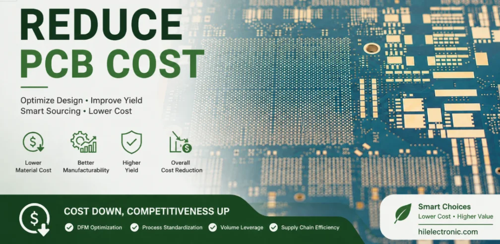
How to Reduce PCB Costs in 2026
On this page Why 80% of PCB Cost Is Locked in at Design...
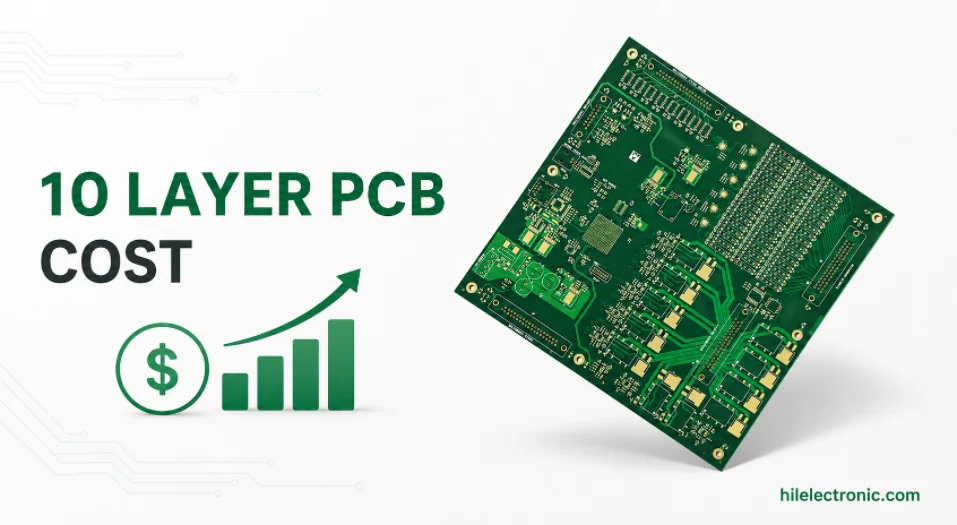
10 Layer PCB Cost Drivers for Materials, HDI and Testing
Figure 1. 10 layer PCB cost drivers for materials HDI and...
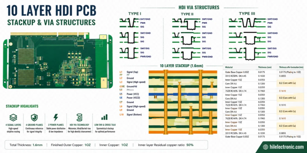
10 Layer HDI PCB Engineering for Microvias and BGA Escape
Figure 1. 10 layer HDI PCB engineering for microvias and...

8 Steps to Manufacture a Perfect Aluminum PCB
Figure 1. Aluminum Pcb manufacturing reference for PCB...
How to get a quote for PCBs
Let us run DFM/DFA analysis for you and get back to you with a report.
You can upload your files securely through our website.
We require the following information in order to give you a quote:
-
- Gerber, ODB++, or .pcb, spec.
- BOM list if you require assembly
- Quantity
- Turn time
In addition to PCB manufacturing, we offer a comprehensive range of electronic services, including PCB design, PCBA (Printed Circuit Board Assembly), and turnkey solutions. Whether you need help with prototyping, design verification, component sourcing, or mass production, we provide end-to-end support to ensure your project’s success. For PCBA services, please provide your BOM (Bill of Materials) and any specific assembly instructions. We also offer DFM/DFA analysis to optimize your designs for manufacturability and assembly, ensuring a smooth production process.