
Micro BGA PCB Assembly Services for High-Density Electronics
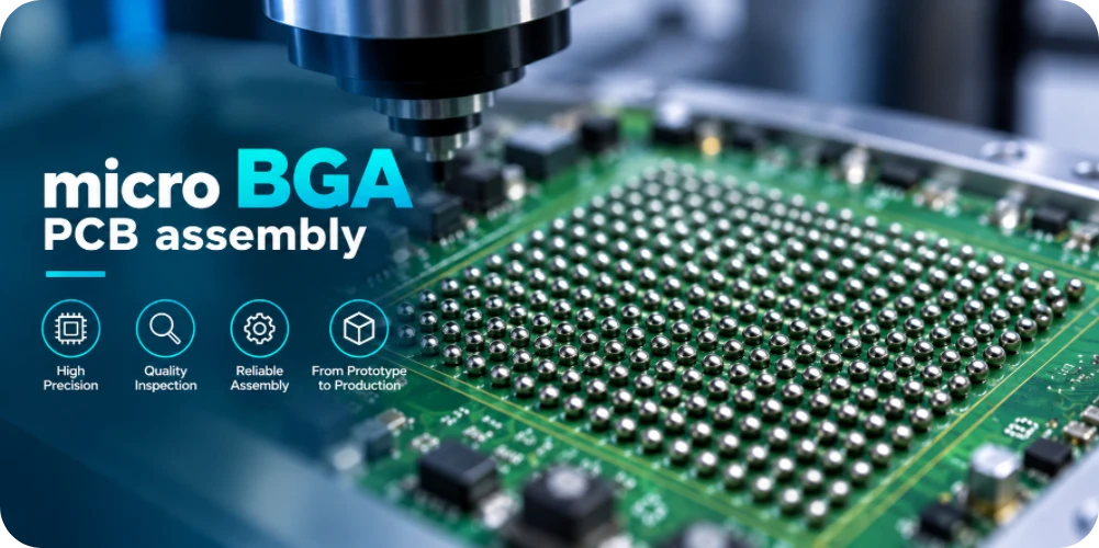
Micro BGA PCB assembly is not simply a smaller version of standard BGA assembly. When the package uses a tight ball arrangement, the manufacturing margin is affected by the PCB footprint, pad geometry, solder-paste deposition, placement alignment, reflow behavior and the ability to inspect joints hidden beneath the package. For a production buyer, the important question is whether the PCB assembly factory can control that entire chain—not merely whether its SMT machine can place the component.
Highleap Electronics is a PCB manufacturing and PCB assembly factory. For micro-BGA projects, the PCB and PCBA can be handled as one manufacturing route, including PCB fabrication, component sourcing, SMT assembly, inspection and agreed testing. This matters when the micro-BGA sits on a dense multilayer board, shares the assembly with other SMT packages, or becomes part of a prototype-to-production program.
A manufacturability review should start with the actual package drawing and released PCB data. The assembly route depends on the micro-BGA ball pitch, package size, PCB land pattern, surrounding components, board construction, stencil requirements, solder materials, reflow conditions and inspection requirements. Highleap’s published assembly information identifies micro-BGA capability, but project acceptance should still be based on the specific package and complete manufacturing data.
Micro-BGA PCB Assembly Requirements for a Production-Ready Build
A micro-BGA assembly should be reviewed from the package outward. The package drawing establishes the ball arrangement and mechanical envelope, while the PCB design determines how the array connects into the rest of the circuit. The assembly process then has to reproduce those interfaces consistently through printing, placement and reflow.
- Package definition: Confirm the exact manufacturer part number, package drawing, ball pitch, ball count, package dimensions and orientation information.
- PCB land pattern: Check the released footprint against the component documentation and the intended fabrication process.
- Array escape: Dense micro-BGA routing may require a carefully selected via and fan-out strategy. The correct solution depends on the package and PCB layer structure rather than on the word “micro-BGA” alone.
- Assembly materials: Stencil, solder paste, solder alloy and reflow requirements should be evaluated together with the board and component population.
- Inspection: Because the solder joints are underneath the package, the inspection plan must include a suitable method for hidden joints.
Which micro-BGA details matter most during the quotation review?
For an assembly quotation, the most useful information is the exact component part number plus the PCB fabrication data and BOM. A generic statement such as “0.3 mm micro-BGA” does not fully describe the manufacturing problem. Two packages with similar pitch can have different ball counts, package dimensions, footprints and board breakout requirements.
For a complete PCB assembly file package, provide the manufacturing files and component information that allow the factory to review the real design rather than estimating from a keyword or package family.
Micro-BGA PCB Layout and Fabrication for High-Density Boards
The assembly process cannot compensate for an unsuitable PCB footprint or an impractical breakout. Micro-BGA projects therefore benefit from treating PCB fabrication and assembly as a connected engineering task. This is especially important when the array forces short escape routes, dense layer transitions or small clearances around the package.
| Design area | What the manufacturer needs to review | Why it affects assembly |
|---|---|---|
| Package footprint | Ball map, pad dimensions, solder-mask definition and component orientation | Determines whether the fabricated land pattern matches the component interface |
| Via and escape strategy | Via location, drill technology, pad clearance and routing around the array | Controls breakout feasibility and available board space |
| PCB stack-up | Layer count, dielectric construction, copper distribution and impedance requirements where applicable | Affects routing, fabrication and thermal behavior during reflow |
| Surface finish | Finish selected for the released PCB and component assembly requirements | Influences the soldering interface and should be considered during process planning |
| Panelization | Panel outline, tooling, fiducials and board orientation | Supports repeatable automated placement and printing |
A PCB DFM review is useful before production because the manufacturing team can examine the PCB data for fabrication and assembly constraints before those constraints become shop-floor problems.
Does a micro-BGA PCB always require HDI?
No. The need for HDI depends on the package, ball pitch, routing density, board dimensions, layer structure and the available breakout method. A micro-BGA may fit on a conventional multilayer construction in one design and require HDI features in another. The correct approach is to evaluate the actual package and routing requirements instead of making HDI a default assumption.
When the released design does require high-density interconnect features, the PCB fabrication route should be reviewed together with the assembly process. Highleap’s PCB fabrication service can be part of that combined manufacturing route.
Micro-BGA Stencil Printing, Placement and Reflow
For micro-BGA assembly, the soldering result is strongly influenced by what happens before the component enters the reflow oven. The stencil aperture, paste condition and printed deposit establish the solder volume available to each site. Placement then has to align the array with the PCB pads, while reflow must produce consistent soldering across the board.
- Review the stencil against the actual footprint. Aperture geometry and foil selection should be considered with the micro-BGA pad arrangement and the other components on the same PCB.
- Control solder-paste printing. Printing variation matters because an abnormal deposit can become a hidden solder-joint issue after the package is placed.
- Verify placement alignment. Vision alignment, package orientation and board fiducials support repeatable placement of the array.
- Profile the reflow process for the actual assembly. PCB construction, solder materials, package characteristics and neighboring components can all affect the thermal profile.
- Inspect the result before release. Visible inspection and hidden-joint inspection serve different purposes and should not be treated as interchangeable.
Why is solder-paste control important for micro-BGA?
The array contains many closely spaced solder interfaces in a small area. Excess or insufficient paste, inconsistent transfer, aperture blockage or print offset can therefore affect multiple joints at once. This is why solder paste inspection is valuable as an upstream process check: it allows printing conditions to be evaluated before the micro-BGA hides the joints.
Can micro-BGA share a PCB with larger SMT and through-hole parts?
Yes. A micro-BGA can be part of a mixed-technology assembly containing other SMT packages and through-hole components. The engineering challenge is to manage the different thermal masses, component clearances, soldering sequence and inspection requirements across the same board. Highleap’s SMT PCB assembly route can be combined with the required through-hole and secondary assembly operations according to the released design.
Micro-BGA PCB Assembly Inspection and Testing
A micro-BGA creates an inspection problem that ordinary optical inspection cannot solve by itself: the solder joints are hidden beneath the package. The inspection plan therefore needs to distinguish between what can be checked optically and what requires a method that can examine the concealed array.
AOI can assess visible component placement and surrounding solder conditions, but it cannot directly see the complete micro-BGA solder array. X-ray inspection is therefore relevant to hidden-joint verification. Electrical or functional testing can provide another layer of evidence, but it does not replace the manufacturing inspection of the solder joints.
- SPI: Evaluates solder-paste deposits before placement and reflow.
- AOI: Checks visible components, placement conditions and accessible solder features.
- X-ray: Provides non-destructive visibility into hidden solder-joint areas beneath the micro-BGA.
- Electrical testing: Electrical testing can verify specified electrical conditions where the design and test method support it.
- Functional testing: Functional testing can be added when the product requires operation-level verification.
Does micro-BGA assembly require X-ray inspection?
For micro-BGA packages, X-ray is commonly used because the solder joints are concealed by the component body. The exact inspection scope should be agreed according to the package, product risk, customer requirements and acceptance criteria. Highleap’s published SMT capability information lists X-ray analysis among its inspection capabilities.
Can a micro-BGA assembly pass AOI and still have a solder-joint problem?
Yes. AOI can identify visible placement and solder-related conditions around the board, but the micro-BGA array itself is beneath the package. A complete quality plan therefore combines the inspection methods appropriate to the accessible and hidden portions of the assembly, followed by electrical or functional testing where required.
Micro-BGA Assembly With Dense SMT, QFN, CSP and Other Packages
A micro-BGA rarely exists alone on a production PCB. It may share the board with QFN, CSP, QFP, connectors, power devices, memory, sensors and conventional chip components. The manufacturing route has to work for the complete component population rather than optimizing one package in isolation.
This is where a PCB manufacturer and assembly factory can offer an advantage over a placement-only supplier. The board construction, pad geometry, panelization and assembly sequence can be reviewed as connected manufacturing decisions. Highleap also provides broader PCB assembly services for prototype and production requirements.
What happens when micro-BGA and QFN are on the same PCB?
The two packages have different solder-joint geometries and thermal behavior. The micro-BGA has hidden array joints, while the QFN has exposed perimeter and thermal-pad requirements. The stencil and reflow strategy should therefore account for both package types and the surrounding component population. A single generic rule for every footprint is not a reliable manufacturing strategy.
For complex boards, the factory can also review the broader PCB assembly manufacturing process so that printing, placement, reflow, inspection and downstream operations remain consistent with the released build.
Micro-BGA PCB Assembly for Prototype, NPI and Production
Micro-BGA programs often become difficult when a prototype process is treated as disposable. A better manufacturing route establishes the package, PCB, stencil, placement, reflow and inspection assumptions early enough that the same engineering logic can carry into NPI and repeat production.
- Prototype review: Confirm package data, PCB files, BOM, assembly drawings and the intended inspection and test scope.
- First build: Verify the actual board, component population, printing, placement and reflow conditions against the released documentation.
- Inspection correlation: Review SPI, AOI, X-ray and electrical or functional results according to the agreed acceptance plan.
- NPI release: Record process changes, approved component substitutions, test requirements and manufacturing notes before repeat builds.
- Production control: Keep the approved manufacturing route stable while controlling changes through the customer’s normal engineering-change process.
How should a micro-BGA assembly supplier support NPI?
The supplier should do more than build the first batch. The useful NPI contribution is a documented manufacturing review that connects the released PCB and BOM to the stencil, assembly program, reflow process, inspection plan and testing requirements. Highleap supports first article inspection and can arrange PCBA prototype builds before production volumes.
What to Send for a Micro-BGA PCB Assembly Quote
A useful RFQ gives the factory enough information to quote the actual manufacturing route rather than a generic assembly price. For micro-BGA boards, the component package and PCB fabrication data are particularly important because the package can influence routing, footprint review, stencil planning and inspection requirements.
- PCB fabrication data: Gerber or other released manufacturing files, stack-up information where required, board dimensions and panelization data.
- BOM: Manufacturer part numbers, quantities, approved alternatives and sourcing requirements.
- Centroid / pick-and-place data: Component locations, rotations and references for automated placement.
- Assembly drawing: Polarity, special assembly notes, mechanical restrictions and component-side information.
- Micro-BGA documentation: Exact part number and package drawing when the package is not sufficiently defined by the BOM alone.
- Inspection and test requirements: X-ray scope, AOI requirements, ICT, functional test or customer-specific acceptance criteria.
- Quantity and build stage: Prototype, NPI, pilot or production volume, plus the required delivery schedule.
What files are needed for an accurate micro-BGA assembly quotation?
The core package is normally the PCB manufacturing data, BOM and placement data, supported by assembly drawings and any package-specific documentation. If the board includes controlled impedance, unusual PCB construction, special surface finishes, testing, coating or other requirements, those should be stated with the RFQ rather than left for production to discover later.
If you already have a complete manufacturing package, you can submit it through Highleap’s quick quote request for project review.
Micro-BGA PCB Assembly FAQ
What is micro-BGA PCB assembly?
Micro-BGA PCB assembly is the process of mounting a micro ball grid array package onto a PCB using an SMT manufacturing process. Because the solder joints are arranged beneath the package, the process requires coordinated control of the PCB footprint, solder-paste printing, placement, reflow and hidden-joint inspection.
Is micro-BGA the same as fine-pitch BGA?
The terms overlap in practical manufacturing discussions, but they should not be treated as interchangeable specifications. The actual package drawing, ball pitch, ball count, package dimensions and PCB footprint determine the manufacturing requirements for a particular device.
What PCB technology is needed for micro-BGA?
There is no single PCB construction that applies to every micro-BGA. Depending on the package and routing density, the design may use conventional multilayer construction, HDI features, microvias or other interconnect strategies. The decision should follow the actual breakout and electrical requirements.
Does Highleap assemble micro-BGA packages?
Highleap publishes micro-BGA assembly capability as part of its PCB assembly offering. Actual production acceptance is based on the specific package, PCB design, component data and manufacturing requirements submitted for review.
Can Highleap manufacture the PCB and assemble the micro-BGA?
Yes. Highleap operates as a PCB manufacturing and PCB assembly factory, so the bare PCB and assembly can be handled within the same manufacturing route. This can simplify coordination when the micro-BGA package requires close alignment between PCB fabrication and assembly engineering.
Can micro-BGA PCBA move from prototype to production?
Yes. The transition is strongest when the prototype build establishes the approved PCB revision, component sources, stencil and assembly process, inspection criteria and test requirements that will be used for subsequent production.

Recommended Posts

Isola Astra MT77 PCB Manufacturing
Figure 1. Isola Astra MT77 PCB ManufacturingIsola Astra...

Nelco N4000-13 PCB Material and Manufacturing Guide | Highleap Electronics
Figure 1. Nelco N4000-13 PCBNelco N4000-13 PCB is a...

Copper Clad Laminate: Complete Material Selection Guide for PCB Engineers
Every electrical property that matters in a printed...

Inside a China Ceramic PCB Factory: Process Control Across Power/LED/RF/Medical
Table of Contents Inside a China Ceramic PCB Factory: How...
How to get a quote for PCBs
Let’s run DFM/DFA analysis for you and get back to you with a report. You can upload your files securely through our website. We require the following information in order to give you a quote:
-
- Gerber, ODB++, or .pcb, spec.
- BOM list if you require assembly
- Quantity
- Turn time
For PCBA services, please provide your BOM (Bill of Materials) and any specific assembly instructions. We also offer DFM/DFA analysis to optimize your designs for manufacturability and assembly, ensuring a smooth production process.