
8-Layer PCB Types: Rigid, HDI, Flex & RF | Highleap
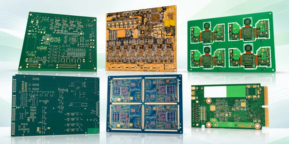
Two 8-layer PCBs can have the same layer count but require completely different manufacturing routes. A standard rigid board, an HDI board with microvias, an all-flex circuit and a rigid-flex assembly are different constructions. RF laminates, heavy copper, controlled impedance and special machining may then be added to those constructions.
Table of contents
- 8-Layer PCB Types by Board Construction
- 8-Layer PCB Variants by Material and Electrical Requirements
- 8-Layer PCB Types with Special Manufacturing Features
- Matching Your 8-Layer PCB Type to the Manufacturing Requirements
8-Layer PCB Types by Board Construction
Rigid 8-Layer PCB
A rigid eight-layer board is the starting construction when the product needs a fixed circuit board rather than a bendable interconnect. Conventional multilayer FR-4 builds usually rely on plated through-holes; advanced vias and low-loss laminates are additional specifications, not automatic features of an eight-layer rigid PCB. To distinguish one rigid build from another, provide the L1–L8 stackup, finished board thickness, copper weight by layer, hole sizes and any tight internal clearances. For a conventional build, Highleap’s multilayer board fabrication capabilities are a useful starting point for matching the design to a production process.
8-Layer HDI PCB
An HDI construction becomes relevant when fine-pitch BGA escape routing or interconnect density requires laser microvias, blind or buried vias, or filled via-in-pad. An eight-layer HDI board might use a 1+6+1 build-up or a more involved sequential-lamination structure; neither is implied by the words “8-layer HDI.” The manufacturing decision depends on which layers each via connects, whether microvias are stacked or staggered, and the required filling and capping. A layer-by-layer via map is more useful than a generic HDI label when checking microvia and sequential-lamination capabilities against the proposed build-up.
8-Layer Flexible PCB
An eight-layer flex circuit is a specialized multilayer polyimide construction. With eight copper layers, the bend region is typically much less compliant than a thin one- or two-layer flex circuit. State whether bending occurs only during installation or repeatedly in service, where the bends occur, which layers pass through those areas, and the coverlay and stiffener arrangement. Bend reliability and finished thickness must be evaluated for the actual construction, particularly when specifying multilayer flexible circuits for a space-constrained product.
8-Layer Rigid-Flex PCB
A rigid-flex board combines rigid component sections and flexible interconnect regions in one construction. “Eight layers” needs a drawing showing the copper-layer count in each zone: an eight-layer rigid section may transition to a flex area containing fewer conductors. The locations of transitions, bend regions, plated holes and assembly components determine the manufacturing approach. The zone-by-zone layer map is also the starting point for reviewing rigid-flex construction and bonding requirements; the maximum layer count alone is insufficient.
8-Layer PCB Variants by Material and Electrical Requirements
The following descriptions are frequently useful to sourcing teams, but they are performance or material specifications applied to a construction rather than mutually exclusive board types.
- High-speed, low-loss 8-layer PCB: Selected when channel loss matters as much as routing density. Identify the laminate grade, relevant Dk/Df data, any insertion-loss target, copper-foil requirements and the controlled signal layers. “High-speed” alone does not specify an acceptable material substitution.
- RF or Rogers/FR-4 hybrid 8-layer PCB: Used where RF circuits require specified low-loss layers alongside other dielectric materials. State exactly which layers use Rogers, PTFE or another RF-grade laminate, along with bondply grades and the intended operating frequencies. The selected dielectric combination must be assessed against the available RF laminate fabrication processes; an eight-layer count does not establish hybrid-lamination feasibility.
- Controlled-impedance 8-layer PCB: An electrical requirement that can apply to rigid, HDI, flex or rigid-flex boards. Identify single-ended or differential impedance targets, tolerances, signal/reference layers, geometry constraints and whether measurement coupons or reports are required.
- Heavy-copper 8-layer PCB: Used for selected high-current paths or power distribution. Specify finished copper weight on each layer, not just “heavy copper PCB.” The factory must review etching clearances, drilling, dielectric thickness and compatibility with fine-pitch signal features against its thick-copper processing capabilities.
- High-Tg or halogen-free 8-layer PCB: These identify laminate restrictions. Supply the specified material grade or applicable material requirements, thermal and reliability constraints, and whether an alternative laminate may be proposed for approval.
If the decision concerns which layers carry signals, ground or power rather than the board construction, Highleap’s eight-layer stackup arrangements address that separate design question. Here, the focus is on manufacturing differences between constructions and material variants.
8-Layer PCB Types with Special Manufacturing Features
Other searches describe an added process rather than the underlying PCB construction. These features can be incorporated into an eight-layer rigid board or, where compatible, another construction:
- 8-layer PCB with gold fingers: For edge connectors, specify contact dimensions, long/short or segmented finger geometry, bevel and selective hard-gold contact plating. A general ENIG note is not a substitute for a defined wear-contact finish.
- 8-layer PCB with controlled-depth cavities or blind slots: Specify machining depth, measurement datum, remaining dielectric thickness and tolerances. The layer count and outline files alone cannot define the machining operation.
- 8-layer PCB with backdrilling: Specify the affected holes, drilling side, drill diameter, intended stop layer and allowable residual stub. These dimensions determine whether controlled-depth via-stub removal can meet the signal-performance requirement.
- 8-layer PCB with edge plating or castellated holes: Identify the exact plated edges or half-hole positions, their copper clearances and surface-finish requirements.
- 8-layer PCB with filled via-in-pad: Identify the via locations, fill and copper-cap specifications, and flatness requirements for the solderable pads. These details matter to both fabrication and BGA assembly.
- Ultra-thin, extra-thick or oversized 8-layer PCB: Define finished dimensions, thickness and flatness tolerances, plus any panel or assembly-handling restrictions. A nominal board size does not establish whether an unusual build is process-compatible.
A board may use several features together, but the combination should be evaluated as a complete stackup and process route. For instance, heavy copper, fine HDI features and a low-loss hybrid laminate each introduce different limitations; approval of each separately does not prove the combined build is feasible.
Matching Your 8-Layer PCB Type to the Manufacturing Requirements
A useful manufacturing description names the construction first, then adds only the requirements that change how that particular board must be built. These examples illustrate the difference:
- Rigid, controlled-impedance: “8-layer rigid FR-4 PCB with specified L1–L8 stackup and controlled differential pairs.” Include copper weights, target impedance and required verification.
- HDI, high-density assembly: “8-layer rigid HDI PCB with proposed 1+6+1 build-up and filled via-in-pad beneath a fine-pitch BGA.” Include the complete via map and fill/cap drawing; confirm the build-up with the manufacturer.
- Rigid-flex, folded enclosure: “8-layer rigid-flex PCB with eight layers in the rigid areas and a separately defined flexible interconnect.” Supply the copper-layer map for each zone and the bend conditions.
- RF hybrid, mixed materials: “8-layer rigid RF/digital PCB with specified Rogers and FR-4 laminate positions.” Include the dielectric schedule, bonding materials, operating-frequency requirements and acceptance targets.
For any of these types, the decisive information is the released stackup, fabrication data, layer-specific copper and material requirements, via connections and drawings for special features. If Highleap will also populate the boards, the same handoff should include the BOM, placement data and assembly and board-level testing requirements.
Highleap Electronics can review the specified eight-layer construction and identify items requiring engineering confirmation. The purpose is to evaluate the actual combination of features, rather than assume that every board described as an “8-layer PCB” follows the same manufacturing route.

Recommended Posts

Quick-Turn 6 Layer PCB Manufacturer in China
Highleap Electronics manufactures six-layer printed...
TG150 PCB Manufacturer for Fabrication and Assembly
Highleap Electronics manufactures TG150 PCB boards to...
TG140 PCB Material Selection and Fabrication
Table of Contents TG140 PCB Materials and Selection...
How to Select Tg180 PCB Materials for Custom Boards
Choosing a Tg180 PCB involves more than selecting a...
How to get a quote for PCBs
Let’s run DFM/DFA analysis for you and get back to you with a report. You can upload your files securely through our website. We require the following information in order to give you a quote:
-
- Gerber, ODB++, or .pcb, spec.
- BOM list if you require assembly
- Quantity
- Turn time
For PCBA services, please provide your BOM (Bill of Materials) and any specific assembly instructions. We also offer DFM/DFA analysis to optimize your designs for manufacturability and assembly, ensuring a smooth production process.