
Embedded Passive PCB Manufacturing for Integrated Designs
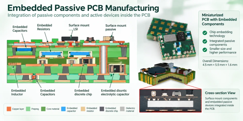
Highleap Electronics provides embedded passive PCB manufacturing project reviews for PCB designs that integrate specified passive functions within the board construction rather than placing every component on the surface. Depending on the required technology, this may involve embedded resistive elements, embedded capacitance or another defined passive structure. If your current supplier cannot support the proposed construction, send us the stackup, electrical targets and material requirements for a feasibility and quotation review.
For embedded passive PCB fabrication, the technology must be identified precisely. Embedded resistor PCB designs and embedded capacitor PCB designs do not use identical materials, geometries or verification methods. Highleap reviews the requested passive type, value and tolerance, layer position, connection details, lamination requirements, test access and programme volume before confirming the project scope.
Table of contents
- What Is Embedded Passive PCB Manufacturing?
- Embedded Passive PCB Fabrication Process for Resistors and Capacitors
- Embedded Passive PCB Design Guidelines and DFM Requirements
- Embedded Passive PCB Cost, MOQ and Lead Time
- Embedded Passive PCB Manufacturer for Feasibility Review and Quotes
- Embedded Passive PCB Manufacturing FAQs
EMBEDDED PASSIVE PCB
- Embedded Passive PCB Manufacturing Services
Request an Embedded Passive PCB Quote →The actual construction, material system, connection method and test access must be qualified for the selected embedded-passive technology.
What Is Embedded Passive PCB Manufacturing?
There are several distinct technologies that all get called “embedded passive”, and they are not variations on the same thing. The classification that matters is where the component’s function comes from.
| Technology | Where the function comes from | How it is made | What you get |
|---|---|---|---|
| Embedded capacitor (buried capacitance) | The dielectric constant of the laminate between two copper planes | A high-Dk, low-loss dielectric layer is used between two internal copper planes; the plane pair forms the capacitor | Very large capacitance in a very small area, with excellent high-frequency behaviour |
| Discreet embedded component | A physical component placed inside the laminate during lamination | The component is placed in a cavity in the prepreg or between prepreg layers, and the stack is pressed around it | A standard component value in a location where surface area was the constraint |
| Printed resistive element | A resistive film deposited between the layers | A resistive paste or film is deposited and fired as part of the layer build | Resistors and dividers in the plane of the board, with no component footprint |
| Embedded inductance | A spiral or coupled structure in the internal layers | Internal copper layers are patterned into a coil | Inductors without a footprint, at the cost of area and Q |
The first row is by far the most common in volume production, because it needs no unusual component supply and no special placement equipment. The second is what most people picture when they hear the term, and it is the most difficult to build, because it requires the component to survive a press cycle and to be connected to copper on both sides.
Embedded Passive PCB Fabrication Process for Resistors and Capacitors
For the discreet embedded component construction, the process sequence is what determines whether the design is feasible. The component is not added to a finished board; it is included in the stack while the stack is being made.
| Step | What happens | What can go wrong |
|---|---|---|
| Cavity creation | A recess is formed in the prepreg or core where the component will sit | Cavity depth and flatness tolerance. If the component sits proud, it will be crushed or will not connect |
| Component placement | The component is positioned in the cavity, often held in place by a carrier film or a fixture | Component displacement during the press cycle, and rotation of a part that is not symmetrical |
| Lamination | The stack is pressed, and the resin flows around the component | Voiding around the component, resin stress on a ceramic or film capacitor, and movement of a part that is not held well |
| Interconnection | Copper is deposited into the recess to connect to the component’s terminals, or the terminals are connected by a separate plating or via structure | Incomplete contact, and the fact that the copper connection to a component terminal is a process in its own right |
| Second-side lamination | Further prepreg and copper layers are built over the embedded layer | Delamination around the embedded component, and additional lamination cycles adding cost and lead time |
Three observations follow from that table, and they explain most of the quotes you will receive.
- The passive structure must be qualified for the full process cycle. Do not assume a standard surface-mount resistor or capacitor can withstand lamination temperature, pressure and resin flow. Suitability depends on the embedding technology, component construction, terminal design, electrical stability and the actual press profile.
- The component has to be placed and held accurately. This is why the design has to define an orientation and, in many cases, a polarity or pin-1 marker.
- The build usually needs more lamination cycles than a normal board. That is where most of the cost and most of the lead time live, and it is why embedded passives are usually specified on boards that are already being built as a build-up structure.
The lamination side of the process is described in our PCB lamination process, and the ways a stackup can be built up in stages are covered in our hybrid PCB lamination. Laminate construction details, including how prepreg and core behave in a press, are in our PCB laminate construction.
Benefits and Limitations of Embedded Passive PCBs
Embedded passives are worth the complexity in a narrow set of situations, and it is worth being honest about the fact that most designs do not need them.
It pays when: the passive count is high and the board area is constrained, so that moving a hundred decoupling capacitors off the surface into the board frees real routing area; the design is high-frequency and the parasitic inductance of a surface capacitor with a via is limiting the performance; the design is a thin or flexing assembly where component height matters; or the design needs capacitance values that are only available as embedded structures, such as a plane-pair capacitance used as a distributed decoupling network.
It does not pay when: the design has a handful of passives and plenty of board area; the programme is low volume and the tooling and setup cost cannot be amortised; the passives need to be individually replaceable or value-trimmed; or the required values and tolerances are widely available in standard surface-mount parts at a lower cost.
A frequent source of confusion is that the buried-capacitance construction and the discreet-embedded-component construction are sold under the same heading but have completely different economics. Buried capacitance is a material decision: you change the laminate and the stackup, and every plane pair in the board becomes a capacitor. Discreet embedded components are a process decision: you add a placement and lamination step to put specific parts inside the board. If a supplier quotes for one while you meant the other, the price difference will be large and the conversation goes badly. This distinction is worth making explicit in the RFQ, and the broader question of what it means to build electronics inside a board is discussed on our embedded PCB structures.
Embedded Passive PCB vs SMT Resistors and Capacitors
| Factor | Embedded passive | Conventional SMT |
|---|---|---|
| Board area used | None, or minimal | A footprint and two pads per component |
| Component height | Flush or near-flush | Full component height |
| Parasitic inductance | Low; the connection is in the plane of the board | Higher; each part needs a via to reach an internal plane |
| Value flexibility | Low; the value is set by the design and the material | High; any catalogue part in any footprint |
| Replaceability | None. A failed embedded part is a failed board | Replaceable |
| Assembly complexity | None at the SMT line; all the complexity is in fabrication | Feeding, placement and inspection of many more parts |
| Cost profile | High setup cost, low marginal cost per unit | Low setup cost, higher cost per part |
That last row is the one that decides most programmes. Embedded passives are a way of converting assembly cost into fabrication cost, and the trade is only worth making when the volume is high enough to amortise the setup.
Embedded Passive PCB Design Guidelines and DFM Requirements
These are the rules that most often force a redesign, and they are worth settling before the artwork is released.
- Component selection. Embedded resistive foils, thin-film resistors, embedded-capacitance dielectric materials and discrete components are different implementation routes. A discrete component must be qualified against the actual lamination profile, pressure, resin system, terminal connection method and post-process electrical limits. Avoid blanket assumptions based on package type or capacitance value; review the specific part number and construction before committing to the design.
- Cavity depth tolerance. The recess has to match the component height closely enough that the terminals connect and the part is not crushed. Height tolerance across a batch of components therefore becomes a design input.
- Placement tolerance and orientation. A non-symmetrical part needs a defined orientation, and the copper that connects to its terminals has to be drawn to the actual position within the process tolerance.
- No rework. A design that needs rework must not put the component inside the board. This also means the assembly test strategy has to change: an in-circuit test fixture may not be able to reach an embedded node.
- Spacing from board edges and vias. The embedded region must maintain the specified clearances to board edges, plated holes and adjacent copper. The required spacing depends on the chosen embedded-passive construction and its lamination or patterning process.
- Value and tolerance statement. The design has to state the target value and the acceptable tolerance, and the fabricator has to state what the process can hold. These are different numbers and they should not be assumed to match.
Because an embedded passive interacts with the stackup, the standard DFM checks still apply and are worth running in full on this design. Our PCB design for manufacturability (DFM) review covers the normal rule set, and the general question of how a stackup should be documented is in our PCB stackup design.
How Embedded Resistors and Capacitors Are Tested
An embedded passive may not be directly accessible for probing after lamination, so test access and the verification strategy must be planned before the stackup is released. Four approaches are used, usually in combination.
- Coupon-based process qualification. A test coupon carrying the same embedded structure is built alongside the panel, and the coupon is measured. This establishes that the process holds the value, without the cost of testing every board. It is the standard approach for a stable production programme.
- Test structures on the panel. Capacitors or resistors of the embedded type are placed in a designated area of the panel and measured. This adds a small amount of area and gives per-panel data.
- Electrical test of the assembled board. The functional performance of the circuit is measured at end of line, which catches a gross error but usually cannot isolate a passive that is slightly out of tolerance.
- Cross-section and microscopy. For development builds, this confirms that the component is properly embedded, that the copper has connected to the terminals, and that there is no voiding around the part.
The distinction that matters in a contract is between per-board measurement and process qualification. A process qualification means the value is controlled by the process and sampled; per-board measurement means every unit is measured, which has a real cost in cycle time. Both are legitimate, but they should be named explicitly in the quotation, because “embedded passives will be verified” is not a specification. The wider options for measuring finished boards are covered in our PCB testing methods.
Embedded Passive PCB Component Sourcing and Qualification
This is the part of embedded passives that most often turns a promising design into a stalled programme, and it is worth working through before quotation.
- The part must be specified exactly. Not “a 100 nF 0402 capacitor” but a manufacturer and part number, because the embedding process has to be qualified against that specific part’s dimensions, its height tolerance and its termination metallurgy.
- Lot control matters more than usual. Because the components are inside the board, a change of manufacturer or a change of production site is a change to the qualified process, and it needs to be controlled rather than treated as a purchasing decision.
- Availability has to be checked before the design is frozen. A component that is only available in a distribution channel on allocation is a risk to the whole programme, and this risk is invisible until the order is placed.
- Qualification is per-construction, not per-part. Once a construction and a component family are qualified, adding another value from the same family is straightforward; adding a different component type is a new qualification. Our electronic component sourcing covers how sourcing and manufacturing are handled together, and the broader approach is described in our sourcing capability page.
Embedded Passive PCB Cost, MOQ and Lead Time
Embedded passives are quoted against a setup cost and a marginal cost, and the difference between the two is large.
The setup cost comes from the cavity tooling, the placement fixture, the process qualification and the material specification. It is paid once, and it is the reason a low-volume programme is rarely economic. Where a design has a modest volume and the same performance can be obtained with fewer surface components, the conventional route is usually the right commercial answer, and a supplier who quotes embedded passives into a 50-piece programme without explaining that trade-off is not being straight with you.
The lead time follows from the process route rather than from the material. Adding an embedded layer generally means at least one extra lamination cycle and an extra build step, and the material may be a non-standard laminate with its own procurement lead time. Our laminate lead time guidance covers the material side of that, and the effect of material choice on the whole board is covered in our PCB materials overview.
The cleanest way to test whether a design is worth the conversion is to cost both versions against the actual programme volume, including the assembly cost saved. That comparison is often decisive, and it is worth asking a fabricator to do it rather than accepting a single price for the embedded option.
Embedded Passive Components vs Embedded Substrates
These two are frequently conflated because both put something inside the board. They are structurally different, and the distinction is easy to miss on a drawing.
- Embedded passive: discrete passive components or a plane-pair capacitance, integrated into the laminate. The board remains one piece. The function lives in the dielectric or in a part inside it.
- Embedded substrate: a separate board or module placed in a recess and interconnected to the host, so the assembly contains an active circuit inside it. This is the construction described on our embedded substrate PCB page.
The choice is usually clear once stated. If the goal is to free up surface area and reduce parasitic inductance, an embedded passive achieves it. If the goal is to integrate a complete module into the board, an embedded substrate is the construction that does it.
Embedded Passive PCB Manufacturer for Feasibility Review and Quotes
For teams searching for an embedded passive PCB manufacturer, Highleap can review the intended embedded structure and the associated PCB fabrication requirements. The RFQ should identify whether the design uses an embedded resistor PCB, an embedded capacitor PCB, buried capacitance, a printed resistive layer or another defined approach. These terms describe different constructions, so a quote should state the proposed technology rather than treat “embedded passive” as a single standard process.
For an embedded passive PCB manufacturing quote, provide the full stackup, material grade, passive values and tolerances, operating voltage or current, temperature and frequency requirements where applicable, connection geometry, test access and quantity. If the project is at prototype stage, specify whether the objective is a feasibility build, engineering sample, qualification lot or production release. The test plan and acceptance limits should be agreed before the first build.
Highleap’s PCB fabrication service is relevant to the overall multilayer board construction, while the PCB DFM review can help identify missing design information before release. For turnkey projects that also include surface-mounted parts, coordinate the BOM and assembly scope through PCB assembly services. The exact embedded technology and qualification requirements must be confirmed against the submitted design.
- Quote package: Gerber/ODB++ files, complete stackup, passive type and values, tolerance, materials, operating conditions, connection details, test plan and expected volume.
Embedded Passive PCB Manufacturing FAQs
Can any component be embedded?
No. The part or passive material must be compatible with the complete lamination cycle, and its electrical connections must remain reliable after pressing. Qualification should use the specific component or material, stackup, lamination profile and test criteria rather than assuming that a whole package category is suitable.
How are the values controlled if they are inside the board?
By the process, and by sampling. A coupon or test structure built with the panel establishes that the process holds the value and tolerance, and the sampling plan is agreed. For a programme where every unit must be measured, that has to be specified, because it changes the cost and the cycle time.
Do embedded passives affect the impedance of nearby traces?
They can. A plane-pair capacitance introduces a shunt capacitance to the planes over that region, which changes the impedance of a trace running above it. If the design has controlled-impedance routing near an embedded capacitor layer, the impedance stackup needs to account for it.
Can an embedded passive board be assembled and tested normally?
Assembly is normal, because there is nothing extra on the surface. Testing needs thought: the embedded component may not be reachable by a test fixture, so functional test or a test structure is usually the answer. If in-circuit test coverage is required, that is a design input and should be settled early.
What if a previous supplier declined the build?
The most common reasons are a genuinely unsupported construction, a component that is not qualified for embedding, or a programme volume below the economic threshold. All three are legitimate. The question worth asking is which of the three it is, because the first is a technical answer, the second is a design change, and the third is a commercial decision. Sending the Gerber, the stackup and the specific part numbers will usually distinguish them quickly.
EMBEDDED PASSIVE PCB · RFQ
Discuss Your Embedded Passive PCB Project
Send the Gerber, stackup, the specific passive part numbers with their values and tolerances, and the programme volume. We confirm the construction, the qualification route and whether the volume supports it.
Part numbers + values + programme volume.

Recommended Posts
Small-Batch High-Mix PCB Assembly for Repeat Orders
Highleap Electronics provides small-batch, high-mix PCB...
EVT DVT and PVT PCB Assembly: From Validation to Production
Highleap Electronics supports EVT, DVT and PVT PCB...
Prototype PCB Assembly: From Design Files to Tested Boards
Highleap Electronics builds prototype PCB assemblies for...
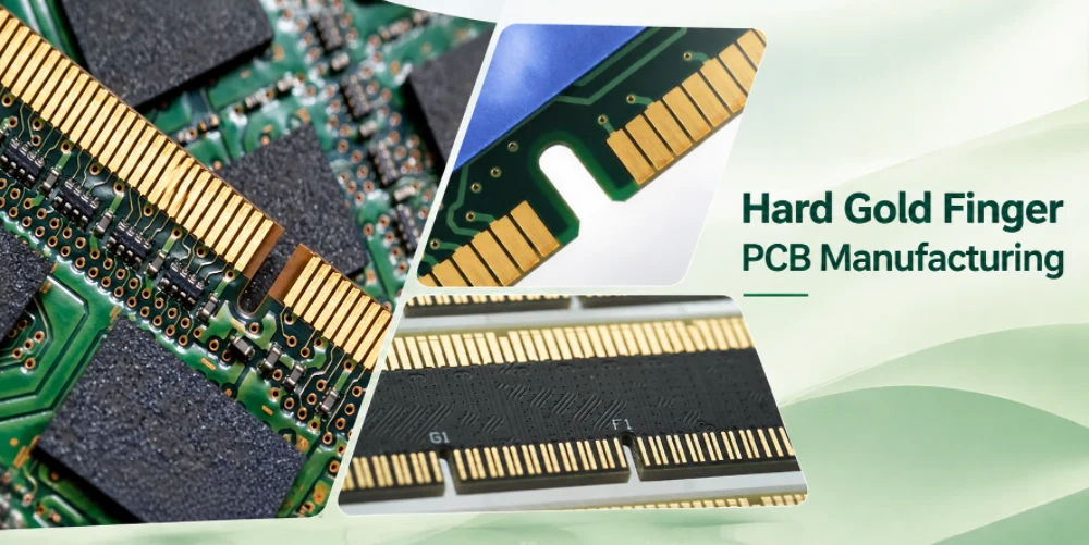
Hard Gold Finger PCB Manufacturing: Plating and Beveling
Hard gold finger PCB manufacturing is used when a circuit...
How to get a quote for PCBs
Let‘s run DFM/DFA analysis for you and get back to you with a report. You can upload your files securely through our website. We require the following information in order to give you a quote:
-
- Gerber, ODB++, or .pcb, spec.
- BOM list if you require assembly
- Quantity
- Turn time
In addition to PCB manufacturing, we offer a comprehensive range of electronic services, including PCB design, PCBA, and turnkey solutions. Whether you need help with prototyping, design verification, component sourcing, or mass production, we provide end-to-end support to ensure your project’s success.
For PCBA services, please provide your BOM (Bill of Materials) and any specific assembly instructions. We also offer DFM/DFA analysis to optimize your designs for manufacturability and assembly, ensuring a smooth production process.