
RO4460G2 Bondply PCB Manufacturing
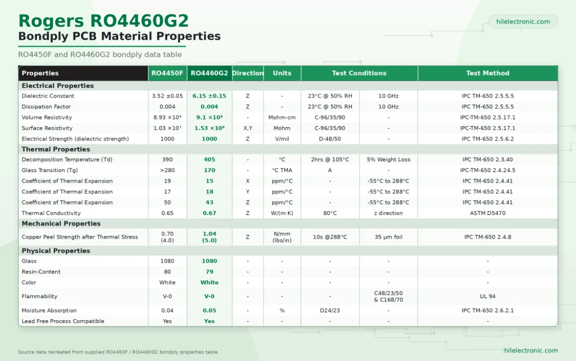
At Highleap Electronics, the engineering review for RO4460G2 is centered on the bonding layer itself. We look at how the bondply participates in the impedance model, whether the chosen cores are electrically compatible, how the lamination cycle affects thickness stability, and where via transitions or cavity features may disturb the RF path. For broader background, see Rogers high-Dk PCB fabrication and high-Dk PCB material.
RO4460G2 bondply is evaluated through its role in a high-Dk multilayer stackup. The manufacturing review connects bondply thickness and lamination behavior with conductor spacing, registration and the final impedance geometry. The bonding choice must also fit Rogers/FR-4 hybrid lamination planning when different core families share the build.
Why RO4460G2 Changes the Stackup Discussion
The bondply is no longer just a bonding film
RO4460G2 bondply is most relevant when a high-Dk multilayer construction needs controlled bonding between RF layers. The useful manufacturing target is the post-lamination geometry, including registration and dielectric thickness. With RO4460G2, the bonding layer can influence the RF geometry in a way that lower-Dk prepregs or bondplies often do not. Designers choose it when miniaturization, coupling behavior, or dielectric matching is part of the electrical target, not simply because the board needs a Rogers-branded adhesive layer.
That changes the fabrication review. The CAM package should not stop at “use RO4460G2.” Highleap needs the intended dielectric thickness, the copper condition used in the field solver, the reference planes involved in the RF path, and the specific layer pairs where the bondply becomes part of the signal environment.
The production risk is usually hidden in the model assumptions
Many problems on high-Dk multilayer RF boards are not caused by the laminate itself. They come from undocumented assumptions: thickness after lamination, finished copper instead of base copper, or a transition from one core family to another without rechecking the impedance calculation. This is why we often cross-check the stackup against PCB impedance control data before quote release.
Where RO4460G2 Works Better Than Lower-Dk Bondply
Compact RF structures are the common driver
RO4460G2 is commonly selected for multilayer microwave boards where the bonding layer must stay closer to the electrical behavior of a high-Dk core. That matters in compact couplers, feed structures, phased RF modules, and high-density front-end boards where routing space is limited.
- Compact RF feed networks with restricted board area
- Multilayer microwave boards using high-Dk cores on adjacent layers
- Filter and coupler circuits where dimensional drift quickly affects tuning
- RF modules that need tighter electrical consistency between prototype and production
Material selection should still be application-driven
RO4460G2 is not automatically the right choice for every Rogers stackup. In some builds, lower-Dk bonding systems are easier to manufacture and fully adequate electrically. In others, the high-Dk bondply supports a smaller RF footprint or a more coherent transition between core layers. The build decision should come from the electrical model and the production tolerance window, not from brand familiarity alone.
Electrical Controls That Matter Before Fabrication
Thickness, copper condition, and reference planes must match the calculation
For RO4460G2, the field-solver assumptions should be treated as manufacturing inputs. If the customer modeled 1 oz finished copper but the stackup note only calls out base copper, the width and impedance expectation can move. The same applies when the reference plane is broken by anti-pads, voids, or split returns near a transition.
| Item | Why it matters | What Highleap checks |
|---|---|---|
| Bondply thickness | Directly affects impedance and coupling | Target thickness, tolerance, press cycle compatibility |
| Copper condition | Changes trace width assumptions | Base copper, finished copper, plating effect |
| Reference plane continuity | Affects return path stability | Plane openings, anti-pad size, transitions |
RF coupons and acceptance criteria should be agreed early
If the build requires coupon validation, phase-sensitive behavior, or specific impedance measurement records, the test method should be stated before fabrication starts. It is better to resolve that at quote stage than to discover after pilot build that the customer expected records that were should not included in the manufacturing package.

Material scope: the Rogers product name is used to identify the laminate specified for the PCB build. Highleap Electronics provides PCB fabrication and assembly, while the laminate is sourced and verified separately.
Lamination and Registration Risks in Production
High-Dk multilayers fail when the press process is treated as routine
RO4460G2 projects usually need more careful lamination review than ordinary FR4 multilayers. The bondply thickness, press flow, and core combination all influence final dielectric height and registration. That is especially important in multilayer RF boards with narrow trace spacing, small couplers, or mixed-material constructions. An evaluation of RO4450F as a distinct bonding material should compare approved press conditions and finished dielectric spacing rather than assume bondply grades are interchangeable.
Highleap evaluates the press sequence, material combination, and panel strategy before release. If the design uses mixed dielectric families, the review also checks whether the stackup would benefit from adjustments seen in hybrid PCB lamination and Rogers PCB stackup planning.
Registration matters as much as dielectric data
In compact RF layouts, a registration shift can disturb reference geometry, via-to-trace spacing, or launch symmetry even when the finished outline looks acceptable. This is why the stackup package should include layer alignment sensitivity if the RF network depends on precise multilayer overlap.
Via Transitions, Assembly, and Reliability Review
Transition design should be reviewed with the laminate, not after it
RO4460G2 boards often include transitions between layers that are electrically sensitive to anti-pad size, ground stitching, and plane continuity. The via structure should be reviewed together with the laminate choice, especially if the board moves between compact RF routing and larger connector geometry.
Assembly planning also matters. If the board includes dense connectors, soldered shields, or grounded metalwork, the heat input and mechanical load around RF areas should be reviewed before finalizing the fabrication drawing. For builds that continue into complete modules, Highleap aligns the board review with RF PCB manufacturing and assembly process capability.
Repeatability is the final filter
The most useful question for sourcing teams is not whether a supplier can make one RO4460G2 prototype. It is whether the same supplier can repeat the thickness, alignment, and transition behavior on the next lot without reopening the whole stackup decision. That is the point where a material-specific PCB manufacturer becomes valuable. Highleap focuses the lamination review on material pairing, press behavior and the alignment of RF features to their reference planes. The bondply cannot be evaluated independently because adjacent core thickness and copper affect the final electrical structure. Exact material property values should be checked against the current supplier documentation for the specified grade and construction.
What Highleap Needs for an RO4460G2 Quote
A complete package shortens the engineering loop
The quickest way to get a reliable quote is to package the electrical assumptions with the board data. For RO4460G2, that usually means more than Gerbers and drill files.
- Released stackup with RO4460G2 thickness and adjacent core callouts
- Impedance table or field-solver targets
- Copper weight, finished thickness, and surface finish
- Via structure notes, especially around RF transitions
- Any coupon, test, or documentation requirement
- Prototype quantity, production quantity, and delivery target
When those items arrive together, Highleap can move faster from material confirmation to manufacturability review and quotation.
FAQs
Is RO4460G2 mainly for size reduction?
Often yes, but not only that. It is usually chosen when the high-Dk bonding layer helps the electrical structure itself, not just the mechanical lamination step.
Can RO4460G2 be mixed with other Rogers core materials?
Yes, but the stackup should be reviewed as a complete electrical and manufacturing system. Mixed-material builds need more documentation than a simple single-family stackup.
Does Highleap need impedance data for every RO4460G2 quote?
If the bonding layer participates in the RF geometry, yes. Even a short impedance table or target model helps prevent avoidable misalignment between design intent and production setup. For quotation, provide the complete stackup, bondply locations, finished thickness, copper and impedance requirements. This lets the supplier calculate the actual lamination route and identify any registration risk before production.

Recommended Posts

Taconic RF 35 vs RO4350B PCB
Table of contentsRF-35 vs RO4350B Procurement and...

TMM4 Filter PCB Manufacturing
TMM4 filter PCB manufacturing is controlled by the...

TMM3 PCB Manufacturing for RF Modules
TMM3 PCB manufacturing is most useful where the RF module...

TMM6 PCB Fabrication
TMM6 fabrication is the process-control page for a mid-Dk...
How to get a quote for PCBs
Let’s run DFM/DFA analysis for you and get back to you with a report. You can upload your files securely through our website. We require the following information in order to give you a quote:
-
- Gerber, ODB++, or .pcb, spec.
- BOM list if you require assembly
- Quantity
- Turn time
For PCBA services, please provide your BOM (Bill of Materials) and any specific assembly instructions. We also offer DFM/DFA analysis to optimize your designs for manufacturability and assembly, ensuring a smooth production process.