
Communication Circuit Board Manufacturing and Assembly Guide

Different Names and Classifications of Communication Circuit Boards
In different countries and industries, communication circuit boards are known by various names. Some common terms include Telecom PCB, Networking PCB, Data Communication PCB, and Wireless Communication PCB. While the terminology may vary, all refer to specialized PCBs designed for reliable signal transmission, protocol management, and system integration. Highleap Electronics is a trusted PCB factory in China, delivering high-quality communication circuit boards for telecom, wireless, and IoT solutions.
Supporting PCBs in Communication Equipment
A communication system never relies on just one PCB. Instead, it integrates multiple specialized boards working together:
- Baseband PCBs – for signal modulation and demodulation
- RF Communication PCBs – for wireless front-end and antenna interfaces
- Power Supply PCBs – ensuring stable voltage and current for all modules
- Control and Interface PCBs – handling user interface, networking, or supervisory control
- High-Speed Backplane PCBs – connecting multiple boards within telecom and data center equipment
These supporting boards form a complete ecosystem, enabling communication devices such as base stations, routers, switches, and satellite systems to function reliably.
Key Design Principles for Communication PCBs
Engineers designing advanced communication PCBs must balance performance with manufacturability. Typical requirements include:
- Multilayer stackups for high-density signal routing
- Controlled impedance for high-speed data transfer
- EMI/EMC suppression through optimized ground planes
- Thermal management to ensure long-term reliability
These factors are especially critical in high-speed communication PCB designs used in 5G, data centers, and aerospace systems.
Material Selection and Performance Optimization
Material selection is one of the most decisive factors in communication PCB design, directly influencing signal quality, reliability, and long-term stability. While cost-effective FR-4 is still widely used for mid-frequency boards, advanced communication systems often require low-loss laminates such as PTFE, Rogers, or hybrid composites to reduce dielectric loss and improve transmission efficiency.
For outdoor wireless communication PCB equipment, materials must withstand humidity, temperature cycling, and UV exposure without degrading electrical performance. In contrast, compact IoT devices prioritize energy efficiency, where dielectric properties affect power consumption and battery life. This has driven demand for IoT-specific PCB solutions that balance low power usage with high-density layouts.
At Highleap Electronics, our manufacturing expertise covers a wide range of laminates, from standard FR-4 to advanced low-loss materials. We provide design-for-manufacturing (DFM) support, ensuring that material choices are compatible with high-layer counts, fine-line etching, and reliable assembly processes, helping customers achieve both performance and cost objectives.

Signal Integrity Challenges and Solutions
Maintaining signal integrity is one of the greatest challenges in communication PCB design. Issues such as crosstalk, reflections, and ground bounce can lead to data loss or instability. Solutions include:
- Differential signaling to reduce EMI
- Proper impedance matching and termination
- Short, well-controlled routing paths
For satellite and aerospace systems, these strategies are mandatory, as even minor signal degradation can cause major system failures. Simulation and validation tools are widely used to predict performance before manufacturing.
Manufacturing and Assembly Excellence
Design precision must be matched by reliable production. At Highleap Electronics, we specialize in communication PCB manufacturing and assembly. Our capabilities include:
- Tight process control for trace width, via placement, and layer registration
- Automated optical inspection and in-circuit testing for quality assurance
- Environmental testing, including thermal cycling and humidity validation
Whether it’s a RF communication PCB for wireless systems or a high-speed data backbone, we ensure every board meets performance and reliability standards.
Applications of Communication Circuit Boards
Communication PCBs are the backbone of a wide range of telecom and networking products. Typical applications include:
- 5G base stations – multilayer PCBs for antennas, RF front-end, and digital processing
- Telecom switches and routers – high-speed backplane PCBs and control boards
- Optical modules and transceivers – precision PCBs for fiber communication
- Wireless access points – RF PCBs with controlled impedance layouts
- IoT devices – compact, low-power boards for smart meters, sensors, and wearables
- Industrial communication systems – rugged PCBs for automation, PLCs, and data acquisition
- Satellite and aerospace equipment – aerospace-grade communication PCBs for harsh environments
- Data center equipment – high-speed server and storage communication boards
Conclusion
Communication circuit boards form the foundation of modern connectivity, enabling everything from global telecom networks to industrial communication systems. Highleap Electronics provides end-to-end PCB fabrication and communication PCB assembly services, ensuring each board is produced with precision, reliability, and scalability. By combining advanced materials, multilayer expertise, and rigorous testing, we deliver manufacturing solutions tailored to the demanding requirements of the communication industry.

Related Articles
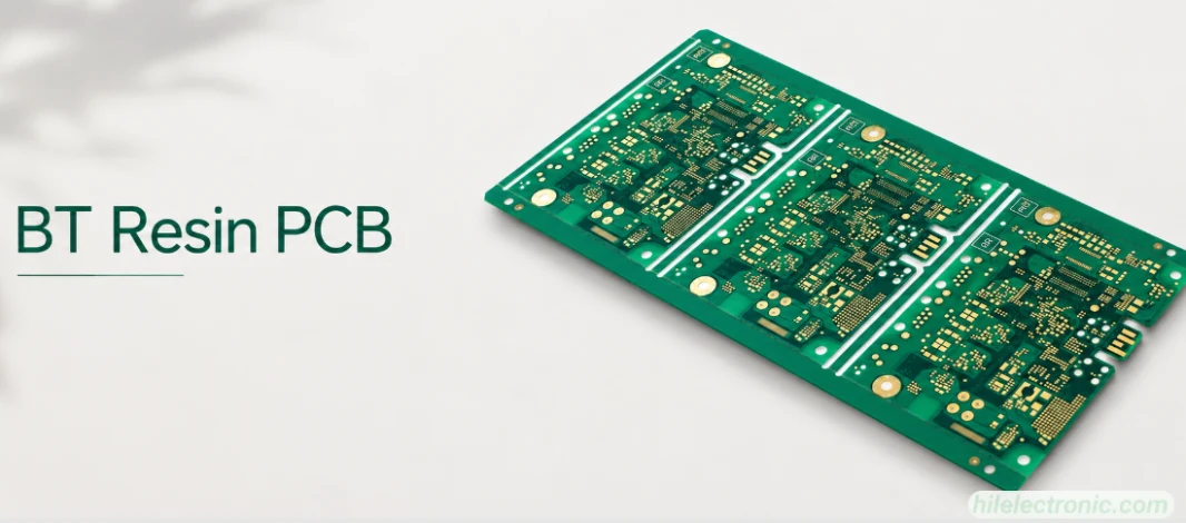
BT Resin PCB: Properties, Uses, and Fabrication Controls
Figure 1. BT resin PCB image for PCB manufacturing...
PCB Potting Services: Compounds, Process, and Design Rules
Figure 1. PCB potting services image for Highleap...
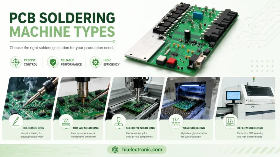
PCB Soldering Machine Types: Reflow, Wave, and Selective Equipment
Figure 1. PCB soldering machine types image for Highleap...

Clean Flux vs No-Clean Flux: Residue, Cleaning, and PCB Reliability
Figure 1. clean flux vs no-clean flux image for Highleap...
How to get a quote for PCBs
Let us run DFM/DFA analysis for you and get back to you with a report.
You can upload your files securely through our website.
We require the following information in order to give you a quote:
-
- Gerber, ODB++, or .pcb, spec.
- BOM list if you require assembly
- Quantity
- Turn time
In addition to PCB manufacturing, we offer a comprehensive range of electronic services, including PCB design, PCBA (Printed Circuit Board Assembly), and turnkey solutions. Whether you need help with prototyping, design verification, component sourcing, or mass production, we provide end-to-end support to ensure your project’s success. For PCBA services, please provide your BOM (Bill of Materials) and any specific assembly instructions. We also offer DFM/DFA analysis to optimize your designs for manufacturability and assembly, ensuring a smooth production process.