
800G Optical Module PCB Manufacturing and Assembly Service
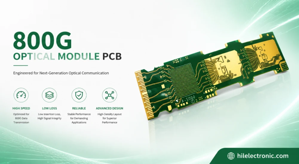
An 800G optical module PCB carries high-speed electrical lanes between the module connector, DSP or retimer, drivers, TIAs and optical engine. In an OSFP implementation, 800G is commonly supported by eight high-speed electrical lanes. The board must preserve insertion loss, return loss, crosstalk and skew inside a very small thermal and mechanical envelope.
Highleap Electronics manufactures the PCB and provides PCB assembly. We do not manufacture low-loss laminate, DSPs, optical engines or transceiver components. We procure and process customer-approved materials and components into finished optical-module PCBAs.
Can Highleap build an 800G optical module PCB? Yes. Send the Gerber files or PCB design files first. A dedicated Highleap engineer will review the high-speed PCB and assembly requirements with our technical team and guide the remaining confirmation one step at a time.
What Makes an 800G Optical Module PCB Different?
The challenge is not the aggregate data-rate label. It is the number of high-speed lanes, per-lane signaling, module form factor, connector launch, trace length, package escape and thermal density. A short module PCB can still be difficult because every via, neck-down, pad and reference transition consumes margin.
Electrical density
Multiple high-speed differential lanes must escape fine-pitch packages and reach the connector with low crosstalk.
Mechanical density
OSFP and related modules impose tight board-outline, component-height and connector-alignment constraints.
Thermal density
DSPs, lasers and drivers create concentrated heat that affects material, copper balance, reflow and warpage.
Optical alignment
Assembly and mechanical references must support the optical engine, fiber interface and housing.
The definition becomes commercially useful when it answers whether the design is manufacturable and what must remain fixed from prototype to production. Material identity, conductor construction, vertical interconnects and mechanical references can all affect the result. Our engineers separate mandatory performance conditions from preferences, then document the manufacturing controls needed for repeat orders.
Material and Copper Requirements for 800G Module PCBs
Material selection must follow channel analysis. Important variables include Df, effective Dk, copper roughness, glass weave, dielectric thickness and material availability. Common solutions use low-loss or ultra-low-loss thermoset systems, often with low-profile copper.
Highleap does not select a material only by published Df. We review the production copper, actual trace geometry, connector loss, via structures and target insertion-loss mask. A premium laminate cannot repair a poor launch or long residual via stub.
Repeatability is the main manufacturing test. A prototype can work even when the process window is broad, but volume production exposes variation in material lots, copper distribution, panel loading and plating. We place low-loss stackup correlation, HDI and via-in-pad process control, tight outline and datum inspection and assembly warpage and X-ray review in the production release to provide a stable comparison between lots.
Design intent and factory compensation have different owners. The customer defines electrical and reliability requirements; Highleap applies the approved CAM, drilling, plating and lamination adjustments needed to reach the finished values. Any change that affects architecture or qualification is raised for approval instead of being hidden inside CAM processing.
800G PCB Stackup, HDI and Routing Priorities
| Design area | Primary risk | Manufacturing response |
|---|---|---|
| Connector launch | Return loss and mode conversion | Anti-pad review, reference continuity and dimensional control |
| BGA escape | Neck-down loss, stubs and crosstalk | HDI/via-in-pad review, laser-drill and plating controls |
| Differential routing | Loss, skew and impedance variation | Controlled stackup, low-profile copper and etch compensation |
| Power delivery | Noise, voltage drop and local heating | Copper distribution, plane design and thermal-via review |
| Board outline | Connector and housing misalignment | Tight datum, profile and final dimensional inspection |
The output of the review should be a buildable stackup and a short list of controlled variables. Highleap documents the agreed material identity, geometry, process route and inspection basis, then coordinates the remaining details internally across CAM, fabrication, quality and assembly.
The stackup must support both escape density and channel performance. Fine-pitch DSP packages may require microvias or filled via-in-pad, while connector-side routing needs continuous reference planes and controlled anti-pad geometry. High-speed pairs should avoid unnecessary layer changes, long stubs and abrupt neck-downs. Power and ground structures also need enough copper without creating excessive thickness imbalance or warpage in the small module outline.
Highleap reviews the actual BGA breakout and connector region before confirming the HDI cycle count. The objective is not to use the most advanced via structure possible, but to use the simplest structure that can meet routing, loss, registration and assembly requirements. This reduces lamination risk and keeps the prototype construction scalable for volume production.
Implications of Using a General-Purpose PCB Process
- Insertion loss may pass simulation but fail on hardware because the copper profile or actual Dk was different.
- Connector launches can dominate return loss even on a very short board.
- Glass-weave-induced skew can reduce margin on long or poorly oriented differential pairs.
- Unfilled or poorly plated via-in-pad structures can create assembly defects beneath BGAs.
- Board warpage can affect fine-pitch packages, optical alignment and housing fit.
- Repeated rework can damage pads, laminate and moisture-sensitive components.
The serious failures usually appear after components have been assembled. A board may pass continuity and still show voids or opens beneath fine-pitch packages, housing or optical-engine misalignment or loss or reflection concentrated at a short launch during system validation. Early DFM is therefore less expensive than investigating a finished PCBA, because material, geometry, fabrication and assembly causes can still be separated before tooling and component placement.
Repeat production creates another risk: a later lot can use a different available construction while the nominal material family remains unchanged. Highleap records the approved stackup, copper, process assumptions and inspection method so prototypes and production are compared against the same release basis.
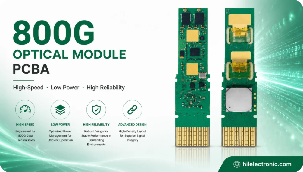
Highleap 800G Optical Module PCB Fabrication Capabilities
Relevant Highleap services include low-loss multilayer fabrication, HDI, sequential lamination, laser drilling, via-in-pad, back drilling, controlled impedance, fine-line imaging, low-loss surface finishes, AOI, electrical test, cross-section and optional S-parameter or insertion-loss testing.
Our public platform capabilities are starting points. The released limits for an 800G module depend on board thickness, aspect ratio, dielectric construction, package pitch, panel design and test coupon requirements.
Different designs require different process windows. Board thickness, material chemistry, copper balance, hole architecture and panel size can change preparation, pressing and plating conditions. The assigned engineer coordinates CAM, production and quality so the customer receives one manufacturing answer instead of separate questions from each department.
The approved manufacturing data are retained for repeat orders. Material identity, scaling, drill route, plating target and inspection method remain under change control. This protects the product from housing or optical-engine misalignment or loss or reflection concentrated at a short launch caused by an undocumented process or supply change.
800G Optical Module PCB Assembly
Highleap supports turnkey and consigned assembly for optical-module electronics, including stencil design, SPI, fine-pitch SMT, BGA/LGA placement, reflow, AOI, X-ray and controlled manual operations. Optical engines, laser components and specialized connectors may require customer-approved handling, fixtures and process instructions.
Assembly review items
- package coplanarity and void criteria;
- moisture sensitivity and bake limits;
- connector seating and mechanical datum;
- thermal-interface materials and heat spreaders;
- cleanliness and flux-residue requirements;
- programming, current draw and functional-test sequence.
The assembly process begins with the bare-board construction. Warpage, copper balance, pad finish, via condition and thermal mass influence printing, placement and reflow. Highleap reviews the PCB and component layout together so a board that meets bare-board tests does not become a low-yield PCBA after high-value parts are loaded.
Turnkey and consigned assembly require different sourcing and traceability controls, but neither should block the initial PCB discussion. The customer can begin with Gerber or design files. BOM, placement and special process data are added when the PCBA scope is confirmed.
Inspection and Test Strategy
Bare-board tests can include 100% electrical test, impedance coupons, microsection, dimensional inspection and optional high-frequency characterization. PCBA inspection can include SPI, AOI, X-ray and functional testing.
A full 800G compliance test normally requires specialized customer or laboratory equipment, fixtures and limit definitions. Highleap can manufacture test coupons and support the agreed test flow, but the acceptance method must be defined before quotation.
The release should state how an out-of-limit result will be investigated. Material records, dimensions, cross-section, plating data and assembly inspection may all be needed. A defined escalation path makes the test actionable rather than collecting measurements with no agreed production response.
Specialized RF or high-speed testing requires defined ports, fixtures, calibration, frequency range and limits. Highleap can support an agreed method, but optional factory characterization is not described as an automatic substitute for the customer’s system compliance or environmental qualification.
The test plan should separate what can be verified on the bare board from what requires an assembled module or specialized fixture. Impedance and microsection data can confirm the stackup and via process, while X-ray and AOI address assembly defects. Insertion-loss or S-parameter measurements require representative coupons and defined ports. A complete 800G module compliance result normally remains dependent on the customer’s system test environment.
Send the Gerber Files First for an 800G Optical Module PCB Quote
Do not wait until every high-speed detail has been organized into a separate RFQ package. Send the Gerber files or the original PCB design files first. If the fabrication notes and stackup are already included in those files, you do not need to prepare them again.
Dedicated engineering support from the first review
A Highleap engineer will work with you one to one and bring the design to our optical-module PCB engineering team. We will review the high-speed routing, HDI structure, via-in-pad, connector area, material, impedance and assembly requirements, then ask only the questions needed to confirm manufacturability, price and lead time. BOM and placement files can be provided later if you also need PCB assembly.
Incomplete early data does not automatically stop the quotation. We identify what is already defined, distinguish preferences from mandatory requirements, and explain which unresolved decision is genuinely blocking. If assembly is required, BOM and placement files can be supplied after the bare-board scope is understood.
800G Optical Module PCB Cost and Lead Time
Major cost drivers include low-loss material, low-profile copper, HDI cycles, filled via-in-pad, fine lines, back drilling, tight profile tolerances, RF coupons, specialized testing and yield. Assembly cost is strongly affected by DSP/optical component procurement, BGA inspection, thermal hardware and test coverage.
For prototype-to-volume planning, yield matters more than unit material price alone. Features that create housing or optical-engine misalignment or crosstalk in dense breakout regions can increase scrap and rework. A stable, documented construction often produces a lower total cost than an aggressive design that requires repeated engineering changes after assembly.
Lead time is often controlled by the exact low-loss construction, special copper availability, HDI lamination cycles and the test method. Component sourcing can become the schedule driver when DSPs, optical engines or specialized connectors are included in turnkey assembly. The assigned engineer identifies the controlling item during quotation and keeps material, PCB and PCBA timing in one project plan.
Build the Complete Electrical, Mechanical and Assembly System
An 800G optical module PCB is not a commodity small board. Highleap combines the approved material, high-speed stackup, HDI fabrication, precision assembly and inspection into one production release.
The PCB, connector, DSP, optical engine, housing and thermal hardware share the same limited space. Treating them as independent purchases creates avoidable conflicts in datum, warpage, component height and reflow exposure. Highleap reviews the bare-board and PCBA requirements together so the released PCB can be assembled into the intended module rather than merely passing standalone electrical test.
The buyer can begin this process by sending the board files. A dedicated engineer becomes the project contact, coordinates the high-speed, HDI, fabrication and SMT teams, and returns the few decisions that need customer confirmation. This service path is more useful than asking procurement to prepare a complete optical-module manufacturing specification before requesting a quotation.
Frequently Asked Questions
Does Highleap manufacture 800G optical transceiver chips or laminate?
No. We manufacture PCBs and PCBAs using customer-approved materials and sourced or consigned components.
Can you build OSFP 800G module PCBs?
Yes, subject to the form-factor drawings, connector, stackup, package escape and DFM review.
Do all 800G boards require ultra-low-loss material?
No. The material should be selected from channel length, topology, copper and loss budget.
Can Highleap perform S-parameter testing?
Optional high-frequency testing can be supported when coupons, ports, fixtures, frequency range and acceptance limits are defined.
Can you assemble DSP and fine-pitch BGA packages?
Yes, subject to package, stencil, warpage, X-ray and reflow review.
What is the fastest way to start an 800G optical module PCB quote?
Send the Gerber files or native PCB design files first. If fabrication notes are already included, no separate document is needed. A Highleap engineer will review the project one to one and coordinate any missing information with our engineering team.
Technical reference note: Material properties and interface descriptions must be checked against the current manufacturer datasheet, customer specification and applicable interface standard for the exact production construction. Highleap Electronics is the PCB fabrication and PCB assembly provider; laminate and component trademarks belong to their respective manufacturers.

Recommended Posts

Isola Astra MT77 PCB Manufacturing
Figure 1. Isola Astra MT77 PCB ManufacturingIsola Astra...

Nelco N4000-13 PCB Material and Manufacturing Guide | Highleap Electronics
Figure 1. Nelco N4000-13 PCBNelco N4000-13 PCB is a...

Copper Clad Laminate: Complete Material Selection Guide for PCB Engineers
Every electrical property that matters in a printed...

Inside a China Ceramic PCB Factory: Process Control Across Power/LED/RF/Medical
Table of Contents Inside a China Ceramic PCB Factory: How...
How to get a quote for PCBs
Let’s run DFM/DFA analysis for you and get back to you with a report. You can upload your files securely through our website. We require the following information in order to give you a quote:
-
- Gerber, ODB++, or .pcb, spec.
- BOM list if you require assembly
- Quantity
- Turn time
For PCBA services, please provide your BOM (Bill of Materials) and any specific assembly instructions. We also offer DFM/DFA analysis to optimize your designs for manufacturability and assembly, ensuring a smooth production process.