
Fitness Tracker PCB Design and PCBA Manufacturing Guide
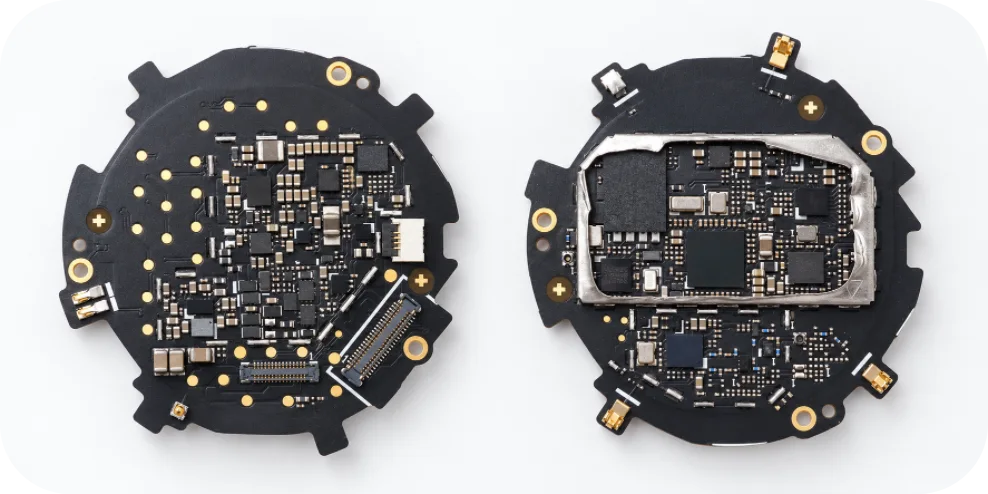
A fitness tracker PCB must combine sensors, Bluetooth PCB connectivity, a display or indicator interface, haptics and battery management PCB in a thin wearable enclosure. The engineering challenge is not any one subsystem; it is making all of them coexist while preserving sensor quality, wireless performance and multi-day battery life. The same PCB may need to support optical PPG, an IMU, flash memory, charging and a vibration motor without allowing those loads to disturb the sensitive measurement path.
Wearable manufacturing also adds mechanical and environmental constraints. The board may be thin, flex PCB or rigid-flex PCB; components may sit very close to the case; sweat and humidity can reach imperfect seals; and the product is charged and worn repeatedly. A successful prototype therefore needs a production plan for sensor alignment, antenna keep-out, fine-pitch SMT, coating or sealing interfaces and functional test.
Highleap Electronics can manufacture customer-designed fitness tracker PCBs and PCB assemblies, source components, assemble fine-pitch packages and flex assemblies when specified, and run customer-defined programming and functional testing. Final biometric accuracy, algorithms and medical or wellness claims remain outside ordinary PCB manufacturing.
Five Engineering Priorities Define a Fitness Tracker PCB
| Priority | Design question | Manufacturing impact |
|---|---|---|
| Miniaturization | How much board area/thickness is available? | Thin multilayer, flex/rigid-flex or HDI PCB only where needed |
| Battery life | What is the real active/sleep duty cycle? | PMIC/regulator BOM, leakage control, current test |
| Sensor performance | Where are PPG/IMU/temperature sensors located? | Placement accuracy, optical/mechanical datums, clean assembly |
| Wireless performance | Where is the BLE antenna relative to wrist/battery/display? | RF keep-out, matching component control, stack-up/ground |
| Wearable reliability | How will sweat, shock, charging and flex affect the assembly? | Coating/masking, connector support, flex strain and final test |
Typical tracker data path
Typical power path
This architecture is different from a smart ring mainly because a wrist tracker usually has more planar area and may include a display. That extra area makes conventional rigid or thin multilayer PCBs more practical, but display connectors, touch interfaces and haptic loads introduce their own routing and power challenges. The correct construction should be chosen from the enclosure and package density rather than assuming every wearable needs rigid-flex or HDI.
The manufacturing package should also define which functions are modules and which are chip-level. A pre-certified BLE module can simplify RF layout at the cost of area; a BLE SoC with PCB antenna can save area but requires tighter reference-layout and matching control. The same trade-off applies to integrated optical sensor modules versus discrete LEDs and photodiodes.
PPG Sensor PCB Layout and Optical Integration
Reflective PPG is widely used in wrist wearables. LEDs illuminate tissue and the photodetector receives the modulated reflected signal. Integrated wearable optical sensors can include LED drivers, analog front end and ADC, but they still depend on physical optics. The PCB sets component position; the enclosure determines skin contact, optical isolation and the light path.
LED-to-photodiode geometry
Spacing and orientation should follow the sensor vendor’s reference guidance and the OEM’s optical design. Moving the sensor to make routing easier can change the measurement path. Board outline and mechanical datums should therefore make the sensor location repeatable relative to the wrist-facing window.
Optical isolation
Direct light leakage from LED to photodiode can reduce useful signal. Mechanical barriers, dark gaskets and molded features often do more than PCB copper. The assembly drawing should still mark optical keep-outs so solder mask, adhesive, coating or nearby reflective components do not intrude into the defined cavity.
Power and ground
LED pulses create current transients that can couple into the analog front end or MCU supply. Local decoupling and return paths should follow the sensor reference design. A battery rail that looks stable at average current may droop during LED pulses or radio transmission, so prototype testing should capture the real active waveform.
Avoid turning a wellness sensor into an unsupported medical claim
PCBA manufacturing can verify sensor communication and a customer-defined optical response. It does not establish clinical accuracy or regulatory status. The article and factory quotation should keep those boundaries clear, especially when the tracker includes SpO2-related optical wavelengths or heart-rate features.
Power Architecture for Multi-Day Battery Life
Battery life is the result of a time-weighted operating profile. A tracker may spend most of its time in low-power sleep, wake periodically to sample sensors, pulse PPG LEDs, refresh the display, log data and transmit over BLE. The design should therefore optimize both quiescent current and the energy of active bursts.
| Load | Power characteristic | Optimization direction |
|---|---|---|
| BLE MCU/SoC | Low sleep current, short RF peaks | Deep sleep, efficient wake/advertising schedule |
| PPG LEDs / AFE | Pulsed optical load | Duty cycle, LED current, sample rate |
| Display | Can dominate active energy | Brightness, refresh rate, display technology |
| IMU / sensors | Often support low-power modes | FIFO, wake-on-motion, duty cycling |
| Vibration motor | High current but short duration | Drive efficiency and event duration |
| Charger / PMIC | Always-connected leakage matters | Low quiescent power and efficient conversion |
Regulator selection
An LDO can provide a simple quiet rail when battery and load voltage are close. A buck or buck-boost converter can extract more usable energy as the battery discharges but introduces switching noise and its own quiescent current. Wearable PMICs may combine charging and multiple rails. The best architecture depends on battery voltage range, sensor sensitivity and duty cycle rather than a universal preference for LDO or DC-DC.
Production current test
Sleep current is a useful manufacturing screen because solder bridges, wrong component values, leakage or firmware configuration can raise it dramatically. The fixture should define the firmware state and settling time. Active-current limits can also be measured during sensor or BLE operation. These tests are more meaningful than checking only that the board powers on.
BLE Antenna Layout, Wrist Loading and RF Keep-Out
A wrist wearable operates close to the body, display, battery and enclosure. These materials influence the antenna. If the tracker uses a PCB antenna, the keep-out and reference ground around it are part of the RF design. A flex tail, metal bezel or battery shift can change tuning even when the radio schematic stays the same.
Follow the radio reference layout
RF PCB layout: the BLE SoC matching network and feed geometry should remain close to the validated reference. Copper pours, vias and test pads added around the antenna can change parasitic capacitance and impedance. DFM should identify the RF zone as design-controlled so manufacturability changes happen elsewhere unless engineering approves them.
Body loading
RF performance should be validated on the assembled wearable or an appropriate fixture because the wrist changes the antenna environment. A bare PCB range test is useful for debug but does not represent final conditions. Production test can screen for missing/misplaced RF components and confirm communication, while full antenna tuning belongs to engineering validation.
Coexistence with display and sensors
Fast display edges and switching regulators can create noise around the radio, while radio bursts can couple into sensitive optical or analog circuitry. Physical placement, reference planes and scheduling can reduce interaction. The exact mitigation is product-specific; the manufacturing job is to preserve the released placement and matching components.
Fitness Tracker PCB Manufacturing & Assembly
Highleap Electronics supports custom fitness tracker PCB and PCBA manufacturing for OEM and product teams, including PCB fabrication, component sourcing, fine-pitch SMT, flex or rigid-flex assembly and customer-defined functional testing. Scale from prototypes to repeat high-volume production with global shipping options, controlled quality checks and responsive after-sales support.
✓ Global Shipping Support
✓ Quality Inspection & Testing
✓ Responsive After-Sales Support
Thin PCB, Flex, Rigid-Flex and When HDI Helps
Fitness trackers can use a thin rigid multilayer board when the electronics fit in the central housing. Flex may connect the display, side buttons, charging contacts or wrist-facing sensor board. Rigid-flex can reduce connectors and thickness where the mechanical architecture benefits. None of these technologies should be assumed solely because the product is wearable.
HDI becomes useful when a fine-pitch BGA or severe area constraint makes standard through-via routing impractical. Microvias and via-in-pad can improve escape density, but they increase fabrication complexity. The design team should compare a slightly larger package or different component placement before committing to HDI purely for fashion.
| PCB choice | Best fit | Key production concern |
|---|---|---|
| Thin rigid multilayer | Centralized tracker body | Warpage, component-to-case height, reference planes |
| Flex tail / flex sensor board | Display, buttons or skin-facing sensors | Bend zones, stiffeners, carrier support |
| Rigid-flex | Connector elimination and folded packaging | Transition reliability, stack-up, panelization |
| HDI | Fine-pitch escape / very high density | Microvia structure, fill/cap, yield and inspection |
Prototype and volume should use the same intended construction as early as practical. A thick rigid evaluation board can prove firmware but reveal little about the antenna, optical alignment or flex strain of the production wearable. Production-intent DVT/pilot hardware is essential before tooling and reliability testing are finalized.
Fitness Tracker PCBA: BGA/QFN/LGA Sensors, Display and Haptics
Wearable assemblies frequently use QFN or BGA MCU/SoC packages, small LGA inertial sensors, optical modules, FPC display connectors and miniature passives. Their assembly risks differ. Bottom-terminated packages need good paste-volume control, while flex connectors need alignment and mechanical support. Optical sensors need clean windows and accurate orientation.
Reflow and moisture-sensitive devices
Component handling should follow manufacturer moisture and reflow requirements. Thin boards can warp during heating, especially when copper distribution is uneven. Panel rails and support fixtures can improve flatness for printing and placement. If a flex section is included, the assembly panel may need temporary stiffening or carrier tooling.
Vibration motor
A haptic motor is electrically simple but mechanically influential. It draws a current pulse and can create magnetic or vibrational interference with sensors. The board and enclosure should route the motor current away from sensitive references and provide strain relief for wires or connectors. Functional test should exercise the motor because a wrong connection can pass all digital sensor tests.
Display connector
FPC orientation is a frequent production risk. Assembly drawings should show the cable insertion side, pin-one and latch position. High-speed display signals should retain their reference path through the connector escape, and DFM should not add large test stubs to timing-sensitive lanes.
Inspection
AOI can screen visible soldering and polarity. X-ray may be used for BGA/QFN/LGA hidden joints when warranted. Optical sensor windows may need a separate contamination check. These inspection steps should be driven by actual package risk rather than listed indiscriminately for every wearable board.
Wearable Reliability: Sweat, Humidity, Shock and Daily Charging
Fitness trackers experience a more aggressive environment than a desktop sensor board. Sweat and condensation can reach the electronics if seals degrade. The unit is dropped, flexed by the wrist, exposed to temperature cycles and charged repeatedly. PCB design and assembly can improve resilience, but the enclosure remains the primary environmental barrier.
Conformal coating
Coating may protect selected circuitry from humidity or contamination, but it must be masked away from connectors, charging contacts, antennas, optical sensors and test points as required. Coating thickness and chemistry can affect rework and RF/optical behavior. It should be specified by the product design, not automatically added because the product is wearable.
Connector and solder-joint support
Charging contacts, USB connectors on some designs and motor wires should be mechanically supported so daily user force is not carried solely by fine solder joints. Flex transitions should avoid sharp bends at stiffener edges. Drop and torsion testing at product level is necessary to validate these structures.
Corrosion and residues
Ionic residues can accelerate corrosion when moisture is present. Cleaning requirements should therefore match the product’s environmental risk and the compatibility of sensors and connectors. A “no-clean” flux designation does not automatically mean the assembly is suitable for every humid wearable application; the OEM should define the acceptable process.
Fitness Tracker PCB Cost Drivers and Prototype-to-Production Planning
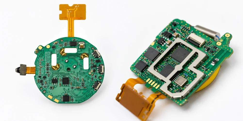
The bare PCB is only one part of wearable cost. Optical sensors, BLE SoC, display, battery, flex construction and test labor can dominate. Cost reduction should therefore consider total assembly and yield rather than forcing the lowest possible layer count.
| Cost driver | Why it increases cost | Cost-down question |
|---|---|---|
| HDI / microvias | Additional fabrication processes | Is the density truly required, or can package/placement change? |
| Rigid-flex | Complex fabrication but removes connectors | Does total assembly/reliability justify it? |
| Tiny packages | More demanding SMT and inspection | Can a larger package fit without enlarging product? |
| Optical sensor / display | High component value | Can sourcing be locked early and alternates qualified? |
| Functional test | Recurring line time and fixtures | Can programming/current/sensor tests be automated? |
| Multiple SKUs | BOM/firmware/test complexity | Can common hardware be preserved with controlled variants? |
Prototype builds should validate optical alignment, BLE performance on the wrist, battery runtime, charging heat, sleep current and enclosure fit. Pilot builds should lock panelization, flex forming, coating/masking, programming and test fixtures. Volume builds then focus on BOM continuity, alternate approval, traceability and process yield.
Approved alternates deserve engineering review because apparently equivalent wearables components can change package height, power consumption, RF behavior or optical response. A controlled alternate introduced during a pilot lot is far safer than an automatic substitution during a volume shortage.
Test time is often an overlooked cost driver. A fixture that programs firmware, measures sleep current, polls sensors, checks charging and verifies BLE in one automated sequence can justify its development cost quickly compared with manual probing of every unit.
How to Choose a Fitness Tracker PCB Assembly Manufacturer
The manufacturing partner should be comfortable with miniature sensor assembly, flex handling and low-power/RF change control, but should not claim responsibility for biometric algorithms or finished-product health accuracy. The best supplier relationship keeps the boundary clear: engineering defines the measurement and RF system; manufacturing preserves the released design and verifies assembly against defined tests.
- Thin multilayer, flex or rigid-flex fabrication matching the released construction.
- HDI/microvia capability when fine-pitch routing truly requires it.
- BGA/QFN/LGA and FPC connector assembly with risk-appropriate inspection.
- Controlled sourcing for optical sensor, BLE SoC, PMIC and RF matching components.
- Programming, sleep-current measurement and customer-defined sensor/BLE functional test.
- Process transfer from prototypes to repeat production with BOM and revision control.
RFQ package
- Gerber/ODB++, fabrication drawing, stack-up and impedance requirements if any.
- Flex/rigid-flex drawing, bend zones and stiffeners when applicable.
- BOM with approved alternates and do-not-substitute sensor/RF parts.
- Pick-and-place and assembly drawings with optical and antenna keep-outs.
- Programming files, firmware/SKU mapping and serial-number requirements.
- Functional-test procedure including current states, sensors, display, haptic and BLE checks.
- Coating/masking or environmental-process instructions when used.
- Prototype, pilot and expected production quantities.
Highleap Electronics can review that package for PCB fabrication, component sourcing and PCBA quotation. The objective is to preserve the validated sensor geometry, low-power architecture, RF layout and assembly process as quantities increase—without adding manufacturing complexity that the product does not need.
Frequently Asked Questions
What PCB technology is commonly used in a fitness tracker?
Thin multilayer rigid PCBs, flex and rigid-flex are all possible. The enclosure, display/sensor interconnect and package density determine the best construction rather than the product category alone.
How does PCB design affect fitness tracker battery life?
Regulator efficiency, quiescent current, leakage, decoupling and power distribution contribute to battery life. Firmware duty cycle, display usage, BLE activity and sensor sampling usually have equally large effects.
What is important in PPG sensor PCB layout?
Preserve LED/photodetector geometry, low-noise power, sensor orientation and optical keep-outs. Final performance also depends on skin contact, optical barriers, windows and algorithms.
Does a fitness tracker always require HDI?
No. HDI is useful when fine-pitch package escape or severe area constraints require microvias. Many trackers can use conventional multilayer or flex construction.
How does the wrist affect BLE antenna performance?
The human body changes the antenna’s electromagnetic environment. Battery, display and enclosure materials also matter, so antenna tuning and validation should use the assembled wearable or an appropriate representative fixture.
What PCBA tests help control battery-life defects?
Defined sleep-current and active-current measurements can catch leakage, wrong parts, solder defects or firmware configuration errors. These complement programming and ordinary functional checks.
What files are needed for a fitness tracker PCBA quote?
Provide Gerber/ODB++, stack-up/flex data, BOM, placement and assembly drawings, antenna/optical keep-outs, programming files, functional-test requirements and build quantities.
Volume Production & Supply Support
For validated wearable designs, Highleap Electronics supports repeat fitness tracker PCB and PCBA production with controlled BOM and revision handling, component sourcing, assembly, inspection and customer-defined testing. Scale from pilot builds to high-volume orders with global shipping options, production quality control and responsive after-sales support.
Manufacturing requirements should be confirmed against the released design files, component manufacturers’ specifications and the end product’s applicable validation or regulatory requirements.

Recommended Posts

TMM4 Filter PCB Manufacturing
TMM4 filter PCB manufacturing is controlled by the...

TMM3 PCB Manufacturing for RF Modules
TMM3 PCB manufacturing is most useful where the RF module...

TMM6 PCB Fabrication
TMM6 fabrication is the process-control page for a mid-Dk...

TMM10 PCB Manufacturing for Compact RF Designs
Table of contentsHow TMM10 Shrinks RF StructuresTMM10 vs...
How to get a quote for PCBs
Let’s run DFM/DFA analysis for you and get back to you with a report. You can upload your files securely through our website. We require the following information in order to give you a quote:
-
- Gerber, ODB++, or .pcb, spec.
- BOM list if you require assembly
- Quantity
- Turn time
For PCBA services, please provide your BOM (Bill of Materials) and any specific assembly instructions. We also offer DFM/DFA analysis to optimize your designs for manufacturability and assembly, ensuring a smooth production process.