
Advanced PCB Manufacturer for Complex and Special-Process PCBs
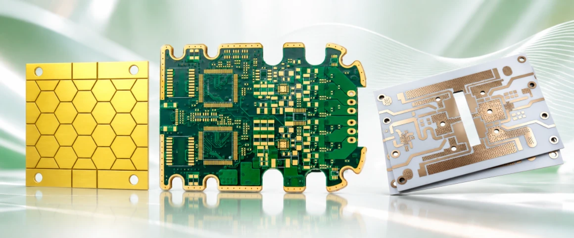
Figure 1. Advanced and High-Complexity PCB Fabrication
Highleap Electronics manufactures rigid, HDI, high-frequency, high-speed, heavy-copper, flex, rigid-flex, metal-core, ceramic and thermal-management PCBs, with PCB assembly available after fabrication. Our advanced manufacturing capabilities cover blind and buried vias, stacked and staggered microvias, resin and copper via filling, VIPPO, back drilling, long-short gold fingers, selective electroplating, controlled-depth slots and cavities, edge metallization, special low-loss laminates, hybrid stackups, copper coins, special finishes and tightly controlled impedance structures.
For boards that combine several advanced requirements, Highleap’s CAM and process engineering teams define one compatible manufacturing route before release. The sequence of lamination, drilling, filling, copper deposition, selective plating, material preparation, solder mask, surface finish, inspection and final machining is planned around the finished PCB requirements so that one special process does not create an uncontrolled conflict with another.
From a conventional multilayer board with one special feature to a high-density build combining HDI, filled vias, backdrill, long-short hard-gold fingers, special RF materials, cavities and tight impedance control, Highleap reviews the complete construction as one manufacturing job. The goal is to preserve the released electrical and mechanical design while converting it into production data, machine programs, process branches and inspection points that can be controlled on the factory floor.
Advanced PCB Manufacturing Capability Matrix
Advanced PCB fabrication covers more than layer count, minimum line width and drill diameter. The following capability families are the structures and processes that can materially change the manufacturing route, equipment sequence, process controls or inspection plan.
| Capability family | Structures and processes | Manufacturing impact |
|---|---|---|
| Advanced via structures | Blind vias, buried vias, mechanical blind vias, laser microvias, stacked/staggered/skip microvias, any-layer interconnect, via-in-pad. | Changes sub-build definition, lamination cycles, drilling method, metallization and registration strategy. |
| Via filling & plugging | Resin plug, non-conductive fill, copper fill, filled-and-capped vias, VIPPO, buried-via fill, microvia fill, solder-mask plugging. | Adds filling, curing, planarization and/or cap plating at specific manufacturing stages. |
| HDI & sequential buildup | 1+N+1, 2+N+2, 3+N+3, any-layer HDI, multiple buildup cycles, stacked via structures. | Repeats lamination, laser drilling, metallization, via fill and imaging rather than relying on one final multilayer lamination. |
| SLP / mSAP | Substrate-Like PCB, modified semi-additive processing, ultra-fine conductors and fine-pitch BGA escape. | Uses thin seed copper and selective conductor buildup rather than conventional thick-copper subtractive processing. |
| Special drilling | Backdrill, multi-depth backdrill, top/bottom backdrill, controlled-depth drill, secondary drilling, press-fit holes, countersink and counterbore. | Adds dedicated CNC programs and Z-axis / finished-hole control. |
| Slots, grooves & cavities | Plated slots, blind slots, controlled-depth blind slots, step grooves, pockets, cavities, plated cavities and semi-metallized depth structures. | Machining may have to occur before metallization, after plating, or in more than one stage. |
| Profiles & panel release | Complex outlines, precision routing, V-score + routing, tabs, bevel/chamfer, step edges and special breakaway structures. | Changes panel support, tool path and the point at which the final outline can be released. |
| Gold fingers | Long-short, staggered, segmented, double-sided and different-length fingers; hard gold; selective gold; bevel/chamfer. | Requires selective electrolytic plating, temporary current paths, masking and controlled final edge machining. |
| Edge metallization | Full/partial/selective edge plating, plated sidewall, ground/shield edge and special edge contacts. | Selected edges must participate in metallization while the board remains supported in the panel. |
| Castellations & plated half holes | Castellated holes, half-moon holes, plated half vias and module-edge castellations. | Uses a drill → plate → route sequence with controlled barrel exposure and edge quality. |
| Special copper plating | Selective extra hole copper, local copper buildup, thick copper plating, via copper fill and project-specific plating routes. | Controls copper thickness locally rather than applying the same copper buildup across the complete surface. |
| Mixed surface finishes | ENIG + hard gold, ENEPIG + hard gold, HASL + hard gold, selective gold and multiple finish areas. | Requires local masking/protection and a controlled order for electroplated and chemical finishes. |
| Special solder mask & functional printing | Peelable mask, fine solder-mask dams, selective mask openings, via plugging/tenting, carbon ink and special protective areas. | Adds dedicated artwork, print/coating, cure and inspection operations. |
| RF & microwave materials | Rogers, PTFE/RT-duroid, Taconic, Arlon, ceramic-filled PTFE and other low-loss RF laminates. | Can change drilling, plasma/surface activation, lamination, copper foil and dielectric control. |
| High-speed digital materials | Megtron, Isola/FR408HR-class, high-speed FR-4, low-loss and ultra-low-loss laminates. | Requires controlled dielectric construction, copper roughness selection and stable high-speed lamination. |
| Hybrid material stackups | Rogers + FR-4, PTFE + FR-4, RF + digital, Megtron + Isola and mixed-dielectric constructions. | Dissimilar materials must be bonded and dimensionally controlled in one multilayer stack. |
| Controlled impedance | Single-ended, differential, tight-tolerance structures, controlled dielectric and TDR coupons. | Links material, pressed dielectric, copper thickness, production trace geometry and electrical verification. |
| Heavy / mixed copper | Heavy copper, thick copper, mixed copper weights, heavy copper + fine line and local thick-copper requirements. | Changes etch compensation, spacing, resin demand and copper balance. |
| Embedded thermal structures | Copper coin, copper inlay, embedded copper slug, heat spreader and thermal via structures. | Adds cavity/inlay machining, metal insertion, resin fill, lamination and planarity control. |
| Metal-core PCB | Aluminum-core, copper-core and insulated metal substrate constructions. | Uses a thermally conductive metal base and dielectric instead of a conventional all-organic multilayer route. |
| Ceramic PCB | Al₂O₃, AlN, Si₃N₄, DBC, DPC, AMB, thick film, thin film, LTCC and HTCC. | Uses ceramic-specific metallization and substrate technologies rather than standard FR-4 fabrication. |
| Flex / rigid-flex | Multilayer flex, HDI flex, rigid-flex, semi-flex, ultra-long flex, ZIF contacts, stiffeners, coverlay and shielding. | Changes material system, lamination, bend-zone construction, reinforcement and handling. |
| Special dimensions | Ultra-thin, thick, long, large-format, narrow-long, irregular and odd-shaped boards. | Changes tooling, support, panel utilization, handling and dimensional control. |
| Special panelization | Custom arrays, step-and-repeat, V-score, routed panel, mixed V-score/routing, breakaway tabs, tooling borders and copper balance. | CAM panel construction becomes part of yield, assembly handling and downstream process stability. |
| Laser processes | Laser drilling, laser microvias, laser cutting/depanelization, laser openings and laser marking where applicable. | Introduces dedicated laser programs and heat/registration controls that differ from mechanical tooling. |
| Special marking | Laser marking, QR/barcode, serial number, date/lot code and permanent identification. | Adds traceability data while protecting contacts, solderable areas and RF structures. |
Advanced Via Structures: Blind Vias, Buried Vias and Microvias
A via becomes an advanced manufacturing structure when its start/stop layers or formation method changes the build sequence. Buried vias are completed in an internal sub-board before later lamination. Blind vias connect an outer layer to a named internal layer and may be mechanical or laser formed. Microvias support dense interconnection and can be stacked, staggered, skip-connected or used as part of an any-layer buildup architecture.
CAM engineering maps every via group to its manufacturing stage. A stack containing L1-L2 laser microvias, L2-L5 buried vias and through holes requires separate data and process stages. The via-span definition therefore belongs to the stackup and production route, not just the finished drill chart.
Highleap’s HDI PCB manufacturing capabilities cover blind/buried vias, microvias, via-in-pad and sequential-lamination constructions.
Via Filling and Plugging: Resin Plug, Copper Fill, Fill & Cap and VIPPO
Via plugging, filling and capping describe different finished conditions. Solder-mask plugging closes or covers the hole as part of the solder-mask process. Resin plugging fills a previously metallized via with a non-conductive resin that is cured and planarized. Copper filling builds copper into the via volume through electroplating. Filled-and-capped vias add a plated surface over the filled structure.
VIPPO—via-in-pad plated over—requires a planarized and plated component land so BGA, QFN and other fine-pitch parts can be assembled directly over the via without an open hole pulling solder away from the joint. When VIPPO appears inside an HDI or sequential-lamination construction, via filling can become part of the buildup cycle before the next dielectric or microvia level is added.
For buried-via structures, resin fill and planarization can also be completed before later lamination. This creates a flatter sub-board surface and prevents the next dielectric from having to bridge open plated holes.
HDI, Sequential Lamination, SLP and mSAP PCB Manufacturing
HDI is a family of buildup constructions rather than one process. 1+N+1, 2+N+2, 3+N+3 and any-layer architectures use one or more cycles of lamination, laser drilling, metallization, via fill and imaging. Stacked microvias require the lower structure to be filled and planar enough to carry the next interconnect level, while staggered designs use lateral offset between buildup layers.
Highleap also supports Substrate-Like PCB manufacturing for higher-density structures. mSAP begins with much thinner seed copper than a conventional subtractive process, selectively builds the conductor, and then removes exposed seed copper by flash etching. This allows finer conductor profiles for dense BGA escape and packaging-like interconnect density.
In both HDI and SLP-style fabrication, the manufacturing architecture is driven by the stackup and via map. Layer count alone does not describe the required process complexity.
Backdrill and Special Drilling Processes
Backdrilling and multi-depth backdrilling
Backdrilling removes the unused plated barrel beyond the last functional via connection. The via is first created and plated as a normal interconnect; the controlled-depth drill then removes the conductive stub from the specified side. High-layer-count high-speed boards can require several backdrill groups with different depths, including top-side and bottom-side operations.
Highleap’s PCB back drilling capability is used for high-speed channels where via-stub control is part of signal-integrity performance.
Secondary / post-plating drilling
Some holes must be created only after an earlier plating or etching operation. CAM places those features in a later drill program so they do not participate in a process that should occur before the final hole exists. The late-stage drilling operation can also be combined with special mechanical or non-metallized features.
Press-fit and precision plated holes
Press-fit connector holes require the finished diameter and hole-wall copper to remain inside a mechanical fit window. Production drill size and plating allowance therefore have to be engineered together rather than checked independently.
Countersink, counterbore and step drilling
Countersinks create a conical recess; counterbores create a cylindrical step. Depth-controlled and step drilling require an explicit reference side, diameter, angle/depth and tolerance. These operations are generated as dedicated CNC programs rather than interpreted from a standard round-hole drill file.
Plated Slots, Blind Slots, Cavities, Pockets and Controlled-Depth Machining
Plated / metallized slots
A slot that requires copper on its walls must be formed before the relevant metallization stage. It cannot be treated as a final profile cut. CAM separates plated slot data from non-plated mechanical slots and checks surrounding copper, tool geometry and downstream routing.
Controlled-depth blind slots and step grooves
Blind slots, partial-depth slots and step grooves are defined in X/Y and Z. The finished drawing should state the reference side, outline, depth or remaining material thickness and tolerance. A step groove may create a mechanical seat, local thickness transition, shielding step, thermal interface or a semi-flex bend zone.
Metallized / semi-metallized controlled-depth structures
If the finished feature requires both a plated region and a later non-plated depth, the route can intentionally split machining into two operations. An initial slot/opening participates in copper deposition; a later controlled-depth milling step creates the final stepped geometry.
PCB cavities and plated cavities
Cavities can recess a component, die, shield or thermal element below the board surface. A non-plated cavity is primarily a precision mechanical operation. A plated cavity requires selected cavity surfaces to participate in metallization and therefore changes the route before final machining. Highleap’s high-frequency PCB manufacturing capability includes plated cavity structures for RF applications.
Special Routing, V-Scoring, Bevels, Step Edges and Complex Board Profiles
Special PCB profiles can combine CNC routing, internal milling, V-scoring, routed tabs, mouse-bites, chamfers, bevels and local step edges. CAM panelization keeps enough mechanical support for plating, imaging, testing and handling before the final outline is released.
Mixed V-score + routed panels are useful when some board edges are straight while other areas require irregular routing. Gold-finger boards can add a controlled edge bevel. Semi-flex or mechanically stepped boards add local depth requirements to the outline program. Very thin, thick or long boards can require additional support and different panel orientation to limit distortion during processing.
Long-Short Gold Fingers, Staggered Contacts and Selective Electrolytic Gold
Long-short, segmented or staggered gold fingers require more engineering than equal-length edge contacts because electrolytic hard-gold plating still needs an electrical current path to every specified finger. CAM may use panel-side plating buses, temporary extensions or another approved connection method depending on the finished geometry.
Those temporary connections have to remain through the selective plating operation and then be removed or isolated during final routing/beveling without changing the customer’s contact length. Double-sided fingers, different gold-thickness zones and restrictions on visible plating leads can add further selective processing.
Highleap’s gold finger PCB manufacturing supports hard-gold edge contacts and dual-finish constructions such as ENIG body + electrolytic hard gold.
Hard gold, soft gold and immersion gold are not interchangeable
Hard electrolytic gold is used for wear-resistant connector contacts. Soft electrolytic gold is used where a different purity or bonding requirement applies. ENIG and ENEPIG are chemical finish systems and should not be treated as equivalent to electrolytic hard-gold finger plating. The manufacturing drawing should identify the finish type, selective area and thickness requirement where critical.
Edge Plating, Plated Slots and Castellated Half-Hole Manufacturing
Edge-plated and castellated features belong to both the electrical and mechanical process. The edge or barrel must exist early enough to be metallized, while the manufacturing panel still needs enough support to survive later operations.
For full or selective edge plating, CAM creates openings that expose only the specified board edges to copper deposition while retaining support tabs or rails. RF modules can combine plated perimeter edges with via fences and plated cavities for shielding and grounding.
Castellated holes follow the essential sequence drill → plate → route through the plated barrel. The final route exposes the plated sidewall as a solderable module connection. Highleap’s castellated PCB manufacturing covers plated half-hole structures used in RF, Bluetooth, Wi-Fi, communication and sensor modules.
Selective Copper Plating and Mixed Surface-Finish Routes
Selective extra hole copper
Where selected plated holes require additional barrel copper without adding the same extra copper to the entire outer surface, the manufacturing route can insert a dedicated temporary resist. The target hole group remains exposed for extra electroplating while the remaining surface is protected, after which the resist is removed and the outer-layer process continues.
Local / thick copper buildup
Local copper build can also be used where defined copper features require additional thickness. This differs from specifying a uniform heavy-copper construction across the full layer because selective plating changes current distribution, resist definition and final geometry.
Mixed and selective surface finishes
One PCB can combine hard-gold contacts with ENIG, ENEPIG, HASL, OSP, immersion tin or immersion silver on other regions. These boards require selective masking and a controlled finish sequence so the first finished area remains protected while the second treatment is applied.
Highleap’s PCB surface finish resource covers ENIG, ENEPIG, immersion silver, immersion tin, HASL, OSP, flash gold and hard-gold plating.
Special Solder Mask, Peelable Mask, Carbon Ink and Protective Processes
Fine solder-mask structures
Fine-pitch BGA and dense SMT designs can require narrow solder-mask dams, selected openings and controlled via tenting or plugging. Via-in-pad structures are treated separately according to whether the via is open, mask covered, resin filled or VIPPO.
Peelable solder mask
Peelable solder mask is a removable protection layer applied only to selected areas. It can protect contacts or keep-out areas during wave/selective soldering, conformal coating or another downstream process and is removed afterward.
Carbon ink and functional printed contacts
Carbon ink can form functional keypad contacts, low-cost switch areas or other conductive/resistive features. It is processed as a functional print layer rather than ordinary legend. The drawing should define the carbon region, and project requirements can include contact resistance, printed thickness or compatibility with the underlying copper/finish.
Protective tape / Kapton masking
Protective tape can be inserted before a thermal, chemical or assembly operation to protect finished contacts or selected surfaces. The application area and the point at which the tape is applied, inspected and removed are defined in the manufacturing traveler.
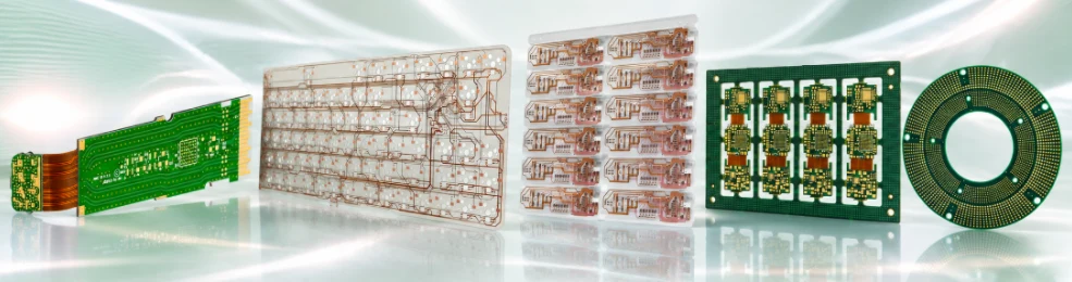
Special Laminates and Hybrid Material Stackups
Highleap manufactures PCBs using RF/microwave, high-speed digital, high-Tg, polyimide and other customer-specified laminate systems. The laminate can change drilling behavior, resin flow, dimensional movement, copper adhesion, surface activation and lamination conditions even when the copper artwork is unchanged.
Rogers, PTFE, Taconic and Arlon
PTFE and ceramic-filled RF materials can require material-specific drilling and hole-wall activation before electroless copper. Highleap’s RF manufacturing content includes plasma treatment and sodium-type surface preparation where applicable. Hybrid RF boards can combine these materials with FR-4 or another low-loss digital laminate.
Megtron, Isola / FR408HR-class and low-loss FR-4
High-speed digital materials are selected for lower transmission loss, controlled dielectric properties and improved thermal performance. Lamination consistency, copper-foil profile and dielectric thickness become important when the board carries multi-gigabit channels and controlled impedance.
N4000-series, IT-150DA, halogen-free and customer-qualified laminates
Customer-approved material programs can require dedicated conditioning or approved fabrication routes. Exact grade availability, permitted equivalents and the qualified process are confirmed before release rather than assuming that every high-Tg or low-loss laminate can use the same generic FR-4 sequence.
For RF-specific fabrication, see Highleap’s Rogers PCB fabrication process.
RF, Microwave and High-Frequency PCB Manufacturer
High-frequency PCB manufacturing combines material control, conductor geometry and special mechanical structures. Highleap supports RF/microwave/mmWave boards using low-loss materials, hybrid stackups, controlled impedance, backdrill, via-in-pad, edge plating and plated cavities.
For RF loss control, copper profile can be as important as nominal copper thickness. VLP, HVLP and other low-profile copper foils reduce roughness-related conductor loss at higher frequencies. Antenna, filter and coupler structures also make manufacturing tolerance part of circuit performance because conductor dimensions and pressed dielectric thickness directly affect the electrical response.
RF boards can also integrate plated cavity structures, perimeter edge plating and dense via fencing for shielding/grounding. These features must be planned before final routing because the metalized surfaces need access to copper-deposition processes.
High-Speed Digital PCB Manufacturer: Backdrill, Low-Loss Stackup and Tight Impedance
High-speed digital boards can combine Megtron/Isola-class low-loss materials, high-layer-count stackups, VIPPO, press-fit connectors, backdrill and controlled impedance. The manufacturing route has to control dielectric thickness, copper thickness, trace geometry, reference-plane relationship and via stub length as one electrical structure.
Highleap’s rigid capability publishes impedance control of ±5 Ω for targets at or below 50 Ω and ±7% for targets above 50 Ω, while supported RF builds can use tighter project-specific control. The accepted target is confirmed with the production stackup rather than taken from one generic percentage.
TDR coupons and test structures verify the produced impedance result. For advanced builds, the coupon represents the actual panel materials, copper and process route rather than only the CAD nominal geometry. See Highleap’s impedance-control PCB manufacturing.
Heavy Copper, Mixed Copper, Copper Coin and Thermal PCB Manufacturing
Heavy copper and mixed copper weights
Highleap’s current rigid capability lists inner and outer copper up to 10 oz for qualified constructions. Heavy copper changes etching, minimum spacing, copper balance and the amount of resin needed to fill the conductor topography during lamination. A mixed stack can use thick power layers and thinner signal layers so high-current and fine-routing requirements can coexist.
See Highleap’s heavy copper PCB manufacturing page for dedicated fabrication considerations.
Copper coin, copper inlay and embedded heat spreaders
Copper coin technology creates a local high-conductivity thermal path beneath a high-power device. The route can include precision cavity machining, copper-piece insertion, resin filling, lamination and planarization. Highleap’s copper coin PCB manufacturing covers embedded and inlay thermal structures.
Metal-core PCB
Aluminum-core and copper-core PCBs use an insulated metal substrate for heat spreading. These are different construction families from heavy-copper FR-4 boards and copper-coin multilayers. Thermal dielectric integrity, electrical isolation, base-metal machining and assembly heat flow are controlled as part of the build.
Ceramic PCB Manufacturer: Al₂O₃, AlN, Si₃N₄, DBC, DPC, AMB, LTCC and HTCC
Highleap manufactures ceramic PCBs using alumina (Al₂O₃), aluminum nitride (AlN) and silicon nitride (Si₃N₄) substrates. The metallization route is selected according to copper thickness, thermal load, conductor density, reliability requirement and multilayer architecture.
DBC directly bonds relatively thick copper to ceramic for power electronics. DPC uses thin-film seed/metallization and electroplating for finer features. AMB uses active-metal brazing for robust metal-to-ceramic bonding. Thick-film and thin-film routes support different conductor technologies, while LTCC and HTCC create multilayer co-fired ceramic structures.
Highleap’s ceramic PCB manufacturing capability also supports downstream assembly processes such as SMT, die attach and wire bonding for applicable projects.
Flex, Rigid-Flex, HDI Flex, Semi-Flex and Ultra-Long Flexible PCB Manufacturer
Flexible PCB and HDI flex
Flexible circuits can use single-, double- or multilayer polyimide constructions with coverlay, ZIF contacts, stiffeners and shielding. HDI flex adds laser microvias, sequential buildup and via filling to the flexible stack.
Rigid-flex
Rigid-flex PCB fabrication integrates rigid and flexible sections into one board. The route controls rigid-to-flex transitions, coverlay, selective bonding, bend regions and final handling. HDI rigid-flex can also combine blind/buried vias, microvias and controlled impedance.
Semi-flex
Semi-flex PCB manufacturing creates a limited-bend zone by controlled-depth milling of a rigid FR-4 structure. The remaining thickness, copper path and milling depth determine the mechanical performance of the bend region.
Ultra-long flex
Highleap’s ultra-long flexible PCB manufacturing addresses meter-scale flexible circuits where handling, registration, voltage drop, lamination and shipping become significant process constraints.
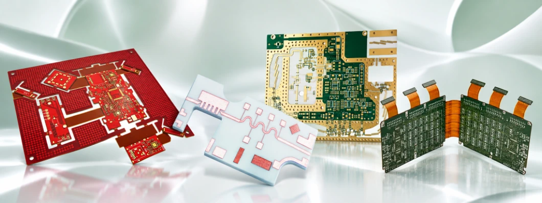
Figure 2. Rigid-flex PCB, ceramic PCB, high-frequency PCB
Special Size, Panelization, Laser Processing and Marking
Ultra-thin, thick, long and large-format boards
Special board dimensions can change tooling, material support, panel layout, dimensional compensation and packaging. Thin panels need additional handling support; thick boards increase drilling/aspect-ratio demands; long and narrow boards can create bow/twist and registration challenges.
Custom panelization
CAM panelization can include step-and-repeat arrays, V-scoring, routed breakaways, breakaway tabs, assembly rails, tooling holes, fiducials, test coupons and copper balancing. Board orientation can also be constrained by flex bend direction, gold-finger plating, material grain or special machining.
Laser drilling, cutting and depanelization
Laser is used for microvias and can also support selected cutting, opening or depanelization tasks where the design and material are suitable. Laser programs require dedicated registration and heat-affected-zone control and should not be confused with LDI, which is an imaging technology rather than laser drilling.
Laser and permanent marking
QR codes, barcodes, serial numbers, date/lot identifiers and other permanent marks can be added for traceability where compatible with the material and finish. Marking location is reviewed so it does not interfere with exposed contacts, RF structures or solderable surfaces.
Embedded and Project-Specific PCB Structures
Some advanced products use embedded copper, heat spreaders, passive structures or other non-standard features inside the PCB construction. Highleap can review customer-specific embedded structures together with the laminate, cavity, plating and assembly requirements.
Embedded resistor, capacitor, inductor or active-component concepts require project-specific confirmation because the material system, process ownership, qualification method and reliability requirements vary significantly. They should not be treated as automatically equivalent to standard multilayer fabrication simply because the feature can be represented in CAD.
Special Verification and Reliability Controls for Advanced PCBs
Advanced manufacturing often requires verification beyond a normal visual inspection. The inspection or test is placed where it can evaluate the relevant structure before a later process hides or changes it.
| Verification | What it evaluates | Typical use |
|---|---|---|
| Inner-layer AOI | Inner conductor opens, shorts and imaging defects | Before lamination buries the inner layers. |
| Outer-layer AOI | Final outer conductor geometry | Before solder mask covers part of the copper. |
| Registration / alignment verification | Layer-to-hole and conductor registration | High-layer-count, HDI and tight hole-to-copper designs. |
| Hole-resistance / special via verification | Electrical performance of specified plated interconnects | Critical through-hole or special interconnect requirements. |
| TDR impedance test | Finished controlled impedance | High-speed and RF transmission-line structures. |
| Microsection / cross-section | Hole-wall copper, via fill, layer interfaces and dielectric construction | HDI, filled vias, high aspect ratio and qualification builds. |
| Electrical continuity / isolation | Finished net integrity | Completed bare PCB. |
| X-ray / hidden-structure inspection | Internal registration or hidden features where applicable | Advanced multilayer / assembly verification. |
| Thermal stress / thermal cycling / IST / CAF | Reliability under thermal or electrical stress | Applied when required by product, customer or qualification plan. |
Highleap’s PCB electrical testing and PCB quality assurance resources cover the broader test and inspection system.
Examples of Advanced PCB Builds with Multiple Special Processes
The manufacturing challenge increases when several advanced structures share the same stackup. Highleap reviews these combinations as one process route so the timing of plating, filling, lamination, finish and mechanical operations remains compatible.
| PCB construction | Processes that must be coordinated | Key manufacturing dependency |
|---|---|---|
| Long-short hard-gold fingers + resin-plugged buried vias + blind/buried vias + controlled-depth blind slot | Sub-board vias, resin fill/planarization, sequential lamination, selective hard gold, plating-current paths and depth-controlled routing. | Buried vias must be filled before the correct lamination; the slot’s plating status sets its machining position; the shorter gold fingers need a viable plating path before final profile release. |
| Rogers/PTFE hybrid + stacked microvias + plated cavity + edge plating + tight impedance | PTFE preparation, hybrid lamination, laser buildup, copper via fill, cavity/edge metallization and TDR verification. | Material, cavity metal, edge metal and impedance geometry all depend on the same pressed construction. |
| Megtron high-speed multilayer + VIPPO + multi-depth backdrill + press-fit connectors | Low-loss stackup, filled/capped vias, controlled-depth drills, precision plated holes and impedance control. | Backdrill must preserve the active layer connection while press-fit holes retain the required finished diameter and barrel copper. |
| Heavy copper power layers + fine-line signal layers + copper coin + filled vias | Mixed copper weights, resin-flow control, copper coin insertion and via fill/planarization. | Heavy-copper topography and coin planarity affect lamination while fine-line layers need a tighter conductor process. |
| HDI rigid-flex + stacked microvias + VIPPO + ENEPIG + controlled impedance | Rigid-flex lamination, coverlay, laser buildup, via fill/cap, finish and impedance stackup. | High-density interconnects must remain compatible with bend zones and still provide flat assembly pads. |
| Castellated RF module + ENIG pads + hard-gold contacts + edge plating | Castellation drill/plate/route, selective hard gold, chemical finish, edge metallization and final profile. | Panel support and temporary plating features must remain until all metalized edge structures are complete. |
| SLP/mSAP + stacked microvias + ultra-fine BGA + low-loss material | Semi-additive conductor formation, fine laser vias, via fill, low-loss stackup and precision registration. | Conductor geometry, dielectric thickness and microvia registration operate inside the same high-density process window. |
| AlN ceramic + DPC fine lines + wire-bondable finish + die attach | Ceramic metallization, fine conductor formation, selective finish and ceramic assembly. | The ceramic metallization and finished metal stack must be compatible with the final die/wire-bond process. |
How CAM Engineering Integrates Special PCB Processes
A special capability becomes useful only when it is placed at the correct point in the manufacturing route. A buried via belongs inside a sub-build. A stacked microvia depends on the fill state beneath it. A plated slot must exist before metallization. A backdrill occurs only after the plated via exists. A long-short gold finger needs its electroplating current path before final routing removes temporary features.
| Finished requirement | Manufacturing definition created by CAM / process engineering |
|---|---|
| Blind / buried via | Via span, sub-build, drilling stage, plating stage and lamination cycle. |
| Stacked microvia | Lower via fill/planarization before the next laser-via level. |
| VIPPO | Fill method, cure, planarization, cap copper and final pad condition. |
| Backdrill | Drill side, target depth/stub, tool diameter and protected connection layer. |
| Long-short gold fingers | Selective area, temporary plating-current path, protection, bevel and lead-removal route. |
| Controlled-depth slot / cavity | Reference side, XY geometry, Z depth/remaining thickness and plating status. |
| Plated slot / edge plating | Pre-plating opening and final panel-support / profile strategy. |
| Selective extra hole copper | Temporary resist and dedicated plating stage for the selected hole group. |
| PTFE / RF laminate | Material-specific drill, bake, plasma/surface preparation and lamination instructions. |
| Hybrid stackup | Material interfaces, bonding system, dimensional compensation and impedance structure. |
| Heavy copper | Etch compensation, spacing review, copper balance and resin-fill strategy. |
| Copper coin | Cavity/inlay geometry, insertion stage, resin fill, lamination and planarization. |
| Mixed finish | Selective masking/protection and finish order. |
| Controlled impedance | Production stackup, compensated conductor geometry, coupon/test data and acceptance target. |
| Rigid-flex / semi-flex | Material transition, coverlay/stiffener, bend region or controlled-depth milling sequence. |
Highleap’s PCB manufacturing process page explains the broader design-to-CAM handoff, while the manufacturing traveler controls how the released job moves through the factory.
Getting a PCB Quote Is Simple
You do not need to prepare a complicated manufacturing package before contacting Highleap. If you already have Gerber files or PCB design/source files, send them to us and our team can start the review. If the design is still being developed, or you are not sure which files are required, simply contact us and send whatever information you currently have.
Our sales and engineering team will help identify the missing information and ask only the questions needed to move the project forward. For PCB assembly, a BOM and placement information are helpful when available, but you can contact us before those files are complete.
- Have Gerber files? Send them.
- Have PCB design files instead? Send those.
- Need PCB + assembly? Add the BOM and placement data if they are ready.
- Files are incomplete or you do not know what to send? Contact Highleap first. Our team will guide you through the next step.
For advanced structures such as blind/buried vias, controlled-depth features, special materials or selective finishes, our engineers may ask for an additional drawing or clarification after reviewing the files. You do not need to understand the manufacturing process in advance; the engineering team will translate the finished requirement into the production route.
Dedicated Project Communication and Order Follow-Up
For active projects, Highleap can organize a dedicated project communication group so the people responsible for the order can work from the same information. Sales, CAM/engineering, production, quality, PCB assembly and logistics team members can join as required by the project.
This gives the customer one place to follow engineering questions, file confirmations, material status, production progress, quality information, assembly issues and shipment updates. If a question appears during CAM review or production, the relevant technical team can be brought into the discussion instead of passing the message through several separate contacts.
Engineering communication
CAM/DFM questions, stackup confirmation, special-process clarification, material substitutions and customer approvals.
Production follow-up
Material preparation, manufacturing progress, key process status and schedule coordination.
Quality follow-up
Inspection findings, engineering disposition, test information and quality documents when required.
PCB assembly & delivery
Component/assembly coordination, production status, final testing, packing and shipment information.
The same project history remains visible to the team throughout the order, which helps engineering decisions, approvals and production updates stay connected to the correct revision and customer requirement.
PCB Manufacturer and PCB Assembly Factory Under One Workflow
Highleap provides both bare PCB fabrication and PCB assembly. This is especially useful for advanced boards because fabrication details can directly affect SMT, through-hole and mechanical assembly. VIPPO affects BGA soldering; press-fit holes affect connector insertion; flex and rigid-flex need suitable support; ceramic and copper-coin boards change thermal behavior; edge connectors and special finishes affect the final mechanical interface.
When fabrication and assembly are coordinated, panel rails, fiducials, via treatment, surface finish, depanelization, keep-outs and test strategy can be reviewed before PCB production is released. Projects that need component sourcing, SMT/THT, programming or functional testing can continue through Highleap’s turnkey PCB assembly workflow.
Project-Specific Confirmation for Non-Standard Structures
Some designs use unusual embedded components, uncommon customer-supplied laminates, special laser-structured features, extraordinary dimensions or combinations outside a standard published capability window. Highleap reviews these projects before production and confirms the applicable material, tooling, equipment and qualification route for the actual design.
Send Your PCB Files to Highleap
Gerber files or PCB design files are enough to start. If your files are incomplete or you are not sure what to provide, contact us and our team will guide the project from engineering review through PCB manufacturing, assembly, quality control and delivery.

Recommended Posts

Kitted PCBA Services for Customer-Supplied Components
Kitted PCBA is a manufacturing model in which the customer...

Build to Print PCB Assembly Services
src="https://hilelectronic.com/wp-content/uploads/2026/08/PC...

Fine Pitch PCB Assembly Services for BGA, QFN & High-Density SMT
If you are sourcing fine pitch PCB assembly, the important...

HDI PCB Assembly | One-Stop HDI PCB Service
Figure 1. HDI PCB Assembly with Black Solder MaskHDI PCB...
How to get a quote for PCBs
Let‘s run DFM/DFA analysis for you and get back to you with a report. You can upload your files securely through our website. We require the following information in order to give you a quote:
-
- Gerber, ODB++, or .pcb, spec.
- BOM list if you require assembly
- Quantity
- Turn time
For PCBA services, please provide your BOM (Bill of Materials) and any specific assembly instructions. We also offer DFM/DFA analysis to optimize your designs for manufacturability and assembly, ensuring a smooth production process.