
Back to blog
Advantages and Applications of Semi-Flex PCB Technology

Semi-Flex PCB
PCBs are integral to the functionality of modern electronics, enabling intricate circuit designs across a myriad of devices from smartphones to aerospace systems. While conventional rigid PCBs dominate the market with their reliability, there exists a growing demand for flexibility in certain applications. This need has propelled the evolution of semi-flex PCBs, striking a balance between rigid and flexible designs to cater to diverse technological requirements.
Understanding Semi-Flex PCBs
Semi-flex PCBs, as the name implies, provide partial flexibility and partial rigidity. They can bend and flex to a certain degree, typically between 30 to 130 degrees, but cannot undergo repeated bending like pure flex PCBs. This semi-flexibility allows for some movement and vibration absorption in the end product while maintaining overall structural stability.
Semi-flexible PCB Materials and Structures
Semi-flex PCBs are made entirely from FR-4 material, making them a cost-effective alternative to flex PCBs. The conductor layers are created by laminating copper foils, usually 1 ounce (35μm) in thickness, onto the substrate. Rolled annealed copper or electro-deposited copper foils are commonly used. A solder mask layer is applied on top to define soldering areas and prevent bridging. Rigid sections of the PCB use typical green solder mask.
These PCBs can integrate 2 to 8 conductive layers, allowing for complex circuit routing similar to multilayer rigid PCBs. Vias and buried vias can connect between layers, and component pads and traces use standard copper or solder finishes like Immersion Tin, ENIG, or OSP.
Advantages and Applications of Semi-Flex PCBs
A semi-flex PCB can only bend in specific areas that have been designed to flex, ensuring it bends only in predetermined ways and at defined points. Except for the flex areas, a semi-flex PCB remains stiff, resembling a traditional rigid PCB. This is achieved through a manufacturing process involving controlled depth routing or milling of the FR4 material on the PCB until it becomes extremely thin and flexible. The flexible section is then treated to prevent cracking, allowing it to bend more freely. Semi-flex PCBs are also manufactured using thin core laminates, with laminates as thin as 0.005 mil utilized for static flex applications. Rolled annealed (RA) copper foils are recommended to prevent cracking and enable a more robust flex.
Semi-flex PCBs are ideal for situations where a PCB needs to be bent only for installation and potential future maintenance. Their flexible nature also makes them a suitable design choice for applications where space is a critical consideration. Common applications of semi-flex PCBs include automotive, industrial equipment, and safety electronics, showcasing their versatility and reliability.
Semi-Flex PCB Comparisons with Other PCB Types
Rigid PCBs: These PCBs are constructed entirely from stiff FR4 material, offering no flex capability. In contrast, semi-flex PCBs feature flexible areas, enabling controlled bending to a certain degree.
Flex PCBs: Utilizing thin plastic films like polyimide, flex PCBs are fully flexible and bendable but lack structural rigidity. Semi-flex PCBs, on the other hand, achieve a balance by providing partial rigidity along with flexibility.
Rigid-Flex PCBs: These PCBs combine rigid and flex boards interconnected through a connector. Semi-flex PCBs, however, integrate both rigid and flex sections within a single board, eliminating the need for a separate connector and providing a more integrated solution.
In summary, while rigid PCBs offer no flexibility and flex PCBs offer full flexibility but lack rigidity, semi-flex PCBs provide a middle ground, offering controlled flexibility along with structural stability. Additionally, semi-flex PCBs provide a more integrated solution compared to rigid-flex PCBs, making them a versatile choice for applications requiring both flexibility and rigidity in a single board.
Semi-Flexible PCB Applications
Semi-flex PCBs, with their unique blend of flexibility and rigidity, are utilized across diverse industries and product categories, including:
Consumer Electronics
- Smartphones and Tablets
- Wearable Devices
- Laptops and Computers
Automotive
- Car Navigation Systems
- Infotainment Systems
- Advanced Driver Assistance Systems (ADAS)
Industrial Automation
- Robotics
- Control Systems
- Sensors and Monitoring Devices
Medical Devices
- Patient Monitoring Systems
- Imaging Equipment
- Wearable Health Devices
Aerospace and Defense
- Avionics
- Communication Systems
- Guidance Systems
In summary, semi-flex PCBs are essential components in a wide array of industries and products, providing the necessary balance between flexibility and rigidity for reliable performance in challenging environments.
Semi-Flexible PCB Design Considerations
To ensure optimal performance and durability of semi-flex PCBs, adherence to specific design guidelines and material specifications is crucial. Parameters such as material processing, routing methodology, bending layer specifications, bending cycle limits, bending radius, and copper thickness on bending layers must be carefully considered and implemented. Additionally, semi-flex PCB design rules related to solder mask, copper clearance, track width, and spacing should be followed meticulously to avoid any potential issues during fabrication and assembly.
Overall, semi-flex PCBs offer a compelling solution for applications requiring flexibility and space optimization. Their cost-effectiveness, reliability, and versatility make them a valuable asset in various industries, driving innovation and efficiency in PCB design and assembly.
The Future of Semi-Flex PCB Technology
Semi-flex PCB technology has seen significant advancements in recent years, primarily driven by the increasing demand for smaller, more flexible electronics. Several key trends are expected to shape the future of semi-flex PCBs:
- Higher Layer Counts: Manufacturing improvements will enable the production of semi-flex PCBs with higher layer counts, exceeding 10 layers. This advancement will facilitate the integration of complex circuits and components.
- Finer Features: Semi-flex PCBs will continue to evolve, approaching the capabilities of rigid PCBs in terms of line and space widths, reaching as low as 2/2 mil, along with 0.1mm vias. This trend will enable further miniaturization of electronic devices.
- Advanced Materials: New substrate materials, such as Liquid Crystal Polymer (LCP), will be utilized for their superior heat resistance and stability. These materials will enhance the reliability of semi-flex PCBs in demanding applications.
- 3D Interconnects: Semi-flex PCBs may incorporate folded or curved 3D shapes to accommodate uniquely shaped electronics. Additive manufacturing techniques will play a crucial role in enabling this 3D integration.
- Design Tools: The development of more sophisticated Computer-Aided Design (CAD) tools will simplify the design process for complex semi-flex PCBs. This will enable faster iteration and prototyping, leading to more efficient development cycles.
- Cost Reduction: Ongoing manufacturing improvements and economies of scale will contribute to lowering the production costs of semi-flex PCBs. This cost reduction will make semi-flex PCB solutions more affordable and accessible.
- Widening Applications: The flexibility and reliability of semi-flex PCBs will drive their adoption in a broader range of cutting-edge applications. From wearables and Internet of Things (IoT) devices to electric vehicles, semi-flex PCBs will play a key role in enabling innovative electronic products.
Overall, the future of semi-flex PCB technology is promising, with expectations of increased versatility, higher performance, and improved cost-effectiveness. These advancements will position semi-flex PCBs as a crucial component in the electronics industry, driving innovation and enabling the development of next-generation electronic devices.
Potential Problems and Solutions During FR4 Semi Flex Fabrication
One of the primary challenges in fabricating FR4 semi-flex boards is ensuring the tolerance and accuracy of depth-control milling to achieve the desired flexibility. Here are some key considerations during the depth-controlling milling process:
Depth-Controlled Milling Test A:
- The manufacturer uses the mapping method for the remaining thickness milling, ensuring the board maintains enough flexibility for a 90-degree bend test.
- Damage to the glass fiber bundle is a common cause of PCB failure.
Depth-Controlled Milling Test B:
- The dielectric thickness of the copper between L2 and the solder mask should be between 0.188mm to 0.213mm.
- Mechanical manufacturing is necessary if the remaining thickness after milling exceeds 0.283mm, with a tolerance of 0.245mm +-0.213mm.
Depth-Controlled Milling Test C:
- Machine uniformity and board warpage can be affected by a forward effect due to size shrinking.
- Milling should be carried out according to the set size of 6.3 X 10.5 inches, with the mapping point measuring the machine uniformity.
Conclusion
Semi-flex PCBs epitomize versatility in modern electronics, bridging the gap between rigid and fully flexible PCBs with finesse. Their ability to offer controlled flexibility alongside structural stability makes them indispensable in industries requiring robust, yet adaptable circuit solutions. As technology continues to advance, further enhancements in materials and manufacturing processes will undoubtedly propel semi-flex PCBs into even more specialized roles, ensuring they remain at the forefront of innovation in electronic design and assembly.

Related Articles
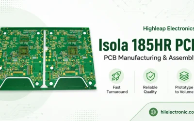
Isola 185HR PCB Manufacturer for High-Reliability Multilayers
Build 185HR automotive, industrial and medical multilayers with controlled lamination, PTH reliability, CAF prevention and assembly verification.
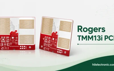
Rogers TMM13i PCB Manufacturer for Ultra-Miniature RF Substrates
Manufacture precision TMM13i substrates for miniature resonators and RF modules with datum control, selective finishes, wire bonding and change control.
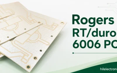
RT/duroid 6006 PCB Manufacturer for Compact High-Dk Microwave Circuits
Produce compact 6006 microwave PCBs with high-Dk geometry control, PTFE processing, temperature validation, tuning and assembly support.