
Alumina PCB Manufacturing for OEM Prototypes and Production
Highleap Electronics provides custom alumina PCB manufacturing for OEMs that need a production partner for ceramic substrates, patterned conductors and, when specified, assembled ceramic electronics. Our manufacturing portfolio includes aluminum-oxide ceramic boards for sensor modules, instrumentation, LED and RF equipment, and hybrid circuits requiring consistent substrate geometry and traceable production releases.
Alumina and Al2O3 are the same material family. This page focuses on manufacturing service delivery: project feasibility, artwork preparation, supplier qualification, prototype runs, repeat orders, inspection, component sourcing and finished assembly—not on repeating a generic material introduction.
Alumina PCB Manufacturer for OEM Ceramic Substrate Supply

Highleap supplies build-to-print alumina ceramic PCBs for electronics developers and equipment OEMs looking for a manufacturing partner. Orders can cover bare patterned alumina circuits, ceramic carriers for later component attachment, or ceramic PCBAs with separately agreed mounting and test activities. Highleap’s ceramic PCB production capabilities include alumina alongside other ceramic substrate families.
A production inquiry should distinguish the required alumina grade, substrate size/thickness, pattern or fired metal system and expected product output. Some OEMs buy a singulated ceramic carrier; others order an array, a solderable ceramic PCB or a board with mounted components. These are different quotation units, cost bases and inspection outputs.
Approved grade, metal system, first-article geometry, test plan and sample identification.
Controlled artwork revision, substrate sourcing, process/inspection route and lot identification.
BOM ownership, mounting method, fixture, environmental requirements and functional-test acceptance.
Can a China alumina PCB supplier manufacture from our existing Gerber files?
Typically yes when the drawing identifies the metallization process and substrate requirements. Ceramic fabrication may require additional DXF, fired-size data, metal-layer definitions or a special drawing for holes and bond pads. A complete dataset is reviewed before tooling or production is committed.
Custom Alumina PCB Fabrication and Metallization Services

Custom alumina PCB manufacturing starts with a controlled substrate and metal pattern rather than a standard FR-4 panel. Highleap can quote ceramic thickness, routing or scribing profile, conductor printing or deposited metal, vias, surface finish and required packaging. Its ceramic substrate fabrication service is a suitable reference for production file review and related inspection operations.
One customer may need 96% alumina with printed conductive and resistive thick-film features; another may use high-purity alumina and a fine-pattern thin-film metal stack. The released manufacturing drawing must identify final conductor thickness and finish, whether dimensions are specified before or after firing, allowable substrate edge condition and the electrical acceptance method. Do not let a generic term such as “alumina PCB” obscure these requirements.
Does every alumina ceramic PCB follow the same manufacturing sequence?
No. A thick-film design requires printed and fired layers; DPC/thin-film metal uses deposition, imaging and plated or etched conductor definition; DBC uses bonded copper foil and subsequent patterning. Ceramic machining can be staged before metallization or, for suitable designs, include post-metallization scribing or separation. The fabrication traveler and inspection gates are agreed for the actual metal system—not borrowed from an ordinary FR-4 PCB sequence.
Do alumina PCB manufacturers offer both thick-film and thin-film options?
These are established ceramic circuit process families, but they must be selected and quoted separately. Thick-film patterns often use fired pastes; thin-film designs use a different deposition and patterning route. Highleap’s thick-film ceramic circuitry offering supports a more specific process discussion.
Alumina PCB Prototypes, Pilot Builds and Small Batches
Alumina PCB prototyping should confirm the ceramic route, not only whether one patterned sample passes electrical continuity. Highleap can review small engineering lots for sensors, medical instrument carriers, LED drivers and precision circuits through its ceramic PCB prototyping and quick-turn planning resources. Actual delivery timing depends on ceramic stock, metallization process, mask/tooling, required test fixtures and approved inspection.
An engineering prototype may use a few ceramic pieces cut from a qualified blank; a pilot order may require array utilization, repeatable film thickness and a packaged lot. If the customer changes the substrate thickness, conductor finish or attach method after prototyping, that is a new manufacturing release, not merely a purchase-order quantity change.
What is the minimum order quantity for an alumina ceramic PCB?
It depends on ceramic stock formats, deposition or printing tooling, panel efficiency and required tests. Highleap can quote the requested sample quantity, but a blanket no-MOQ promise for every ceramic process would be misleading. Include a production forecast so NRE and material minimum-buy assumptions are transparent.
Thick-Film, Thin-Film and Direct-Copper Alumina Circuits

Highleap’s alumina manufacturing service can be scoped for hybrid thick-film electronics or precision patterned ceramic boards. The manufacturing route follows the specified circuit rather than an assumed default finish. Thin-film alumina builds may require finer geometry and a metal stack compatible with solder or wire bonding; thick-film builds may need fired conductor/resistor pastes, crossovers and additional screen-print steps.
| Alumina project | Typical production focus | Customer-supplied specification |
|---|---|---|
| Printed thick-film hybrid | Paste system, firing route, optional printed resistor and passivation. | Ink family, trim/tolerance, circuit image and acceptance. |
| Thin-film alumina carrier | Metal deposition and fine-pattern features with specific finish. | Metal stack, line/space, substrate surface, bond/solder pad requirement. |
| Copper-metallized power alumina | Copper-to-ceramic bond and thermal/electrical isolation. | Copper geometry/thickness, voltage clearances, thermal interface. |
For fine-feature work, see Highleap’s thin-film patterned ceramic circuit services. A buyer should also check whether plated through features, singulated geometry, special substrate polish or bond-pad inspection are in the base quote or separate NRE. Treat different metal processes as different specifications even when they use the same alumina grade.
Printed conductor/resistor pastes with a firing and, if specified, trimming acceptance plan.
Patterned metallization with specified line/space, metal thickness, adhesion and bondable or solderable finish.
Bonded copper, isolation requirements and etched geometry defined by the power circuit.
Can one supplier build both the alumina circuit and the finished module?
This is possible when ceramic manufacturing and the particular assembly route are both scoped. Wire bonding or die attachment needs its own process, tooling and acceptance definition; it is not automatically included merely because the supplier also has conventional SMT machines.
Alumina Circuit Boards for Sensors, LEDs and Hybrid Electronics
Alumina ceramic PCB manufacturing serves applications where insulation, stable substrate geometry and compatible patterned metal are important. Highleap can discuss industrial sensor electrodes, temperature and pressure measurement modules, RF hybrid circuits, LED carriers, optoelectronic modules, test instruments and high-temperature control electronics. Exact fit depends on the electronic design and package, not on a universal “ceramic is better” statement.
If product heat flux is substantially higher, the buyer may need aluminum nitride rather than alumina, or a separate ceramic system with different thermal properties. Highleap’s ceramic-base PCB material and integration overview provides context for these choices; the final thermal specification must be verified against the actual device and mounting stack.
Is alumina PCB manufacturing suitable for high-power LED products?
It can be appropriate for certain LED packages and driver assemblies. Compare the target junction temperature, total heat path, substrate grade and cost. Alumina does not have the same bulk thermal conductivity as high-grade AlN, and the complete module requires thermal verification regardless of material choice.
Alumina PCB Assembly, Component Sourcing and Module Integration

Highleap can coordinate alumina ceramic PCB fabrication with approved component procurement and project-specific assembly. For compatible projects, the commercial package may include solderable or bondable ceramic circuits, component sourcing, SMT placement, dedicated die-attach/wire-bond operations and electrical inspection. The one-stop PCB assembly and integration service provides the broader PCBA infrastructure; specialized ceramic attach capability and test responsibilities must be confirmed for the nominated order.
If the customer supplies a proprietary sensor die, optical emitter or critical IC, the receiving and stock ownership rules must be established just as they would be for conventional PCBA. Highleap’s electronic component sourcing support can be included for the remaining approved BOM. Do not silently replace ceramic substrate grade, bond metal or die variant to solve a purchasing shortage.
Are ceramic die attach and wire bonding included in standard PCB assembly?
No. They are specialist operations with separate fixtures, material controls and bond/attach qualification. Where requested, Highleap can assess a coordinated package and state which facility or qualified partner performs the operation. Gold wire bonding requires an approved bondable surface rather than automatic specification of wear-resistant hard gold.
Can Highleap provide assembled alumina PCBAs with functional testing?
Yes, subject to the parts, process route, fixture and customer pass/fail procedure. Ask whether every unit, a defined sample or a separate qualification lot is tested. Bare ceramic electrical continuity is not equivalent to verified performance of a populated sensor or LED module.
Alumina PCB Production Quality, Inspection and Traceability

Consistent alumina PCB supply depends on controlled materials, manufacturing route and acceptance data. Highleap can agree substrate grade certificates, drawing-revision control, visual/dimensional checks, metal pattern inspection, electrical tests and special reliability records. The PCB inspection and quality information is a useful adjacent service reference, but every ceramic program needs its own criterion set.
For repeated orders, the OEM should define whether a lot corresponds to a ceramic substrate supplier batch, a printing or plating run, a singulation batch, or the final assembly configuration. Important change triggers may include substrate grade or supplier, metallization paste or metal stack, fired dimension compensation, final surface finish and attachment process. A repeat purchase based solely on an unchanged part number can hide meaningful manufacturing changes.
Alumina grade and approved blank specification
Drawing revision and conductor/finish route
Dimensional, pattern, edge and electrical results
Lot identity, quantity, packaging and exceptions
Must every ceramic board receive the same electrical and reliability tests?
No. The design defines whether continuity/isolation applies, whether breakdown testing is acceptable or destructive, and whether adhesion, thermal cycling or other screening is required on samples or the lot. Write the sampling plan and report deliverables into the order to prevent a generic inspection statement from being mistaken for completed qualification.
How should alumina PCB lots be identified for repeat OEM production?
Use the customer part and revision, manufacturer lot, specified substrate material lot where required, process/finish revision and acceptance record. For assembled boards, add firmware or configuration information if relevant. Agree retention and shipment-label format before placing recurring orders.
Alumina PCB Manufacturing Quotes, MOQ and Lead Times
A reliable alumina PCB manufacturing quote must identify the ceramic grade and the exact deliverable. Material size, thickness, blank yield, conductor method, plating/printing steps, fired or precision dimensions, special inspection and requested lot size all influence production price. Assembly adds component purchasing, fixtures, attachment, test and packing charges. Highleap’s ceramic PCB procurement and sourcing guidance is relevant when comparing offers for a recurring supply program.
- Fabrication package: 96%/99.6% alumina grade, supplier restrictions, finished drawing, Gerber/DXF, hole map and metal system.
- Acceptance: continuity/isolation, dimensions, edge condition, film/bond evidence and documentation requirements.
- Assembly: BOM and sourcing responsibility, solder/die attach or wire bond steps, fixtures and functional-test criteria.
- Ordering: first-article and recurring lot quantities, forecast, packaging, destination and part lifetime expectations.
Highleap also provides ceramic manufacturing supplier evaluation information for OEMs assessing process compatibility and supply reliability. Request the finished-board price and any tooling, test, packing or specialist-process costs as separate line items to avoid comparing incompatible quotations.
What actually controls alumina PCB manufacturing lead time?
Substrate grade and blank availability, artwork preparation, fired/metal deposition cycles, machining or post-metallization singulation, required plating and lot acceptance can each be the critical path. A promised universal two-week route would ignore these differences. Highleap can review the exact ceramic drawing, quantities and assembly/test scope before providing a project-specific production schedule.
What is the typical lead time for alumina PCB manufacturing?
There is no single reliable number across thick-film, thin-film and copper-bonded alumina boards. Time depends on ceramic blank availability, masking/tooling, metal processing, firing or plating, singulation, inspection and any component delivery. Ask for a scheduled plan tied to approved documents and confirmed material, not a generic assembly-only estimate.

Recommended Posts
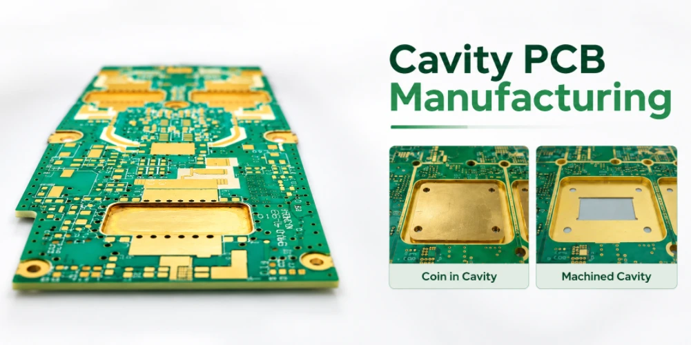
Special-Feature Circuit Boards for OEM Products
Highleap Electronics / PCB + PCBA...
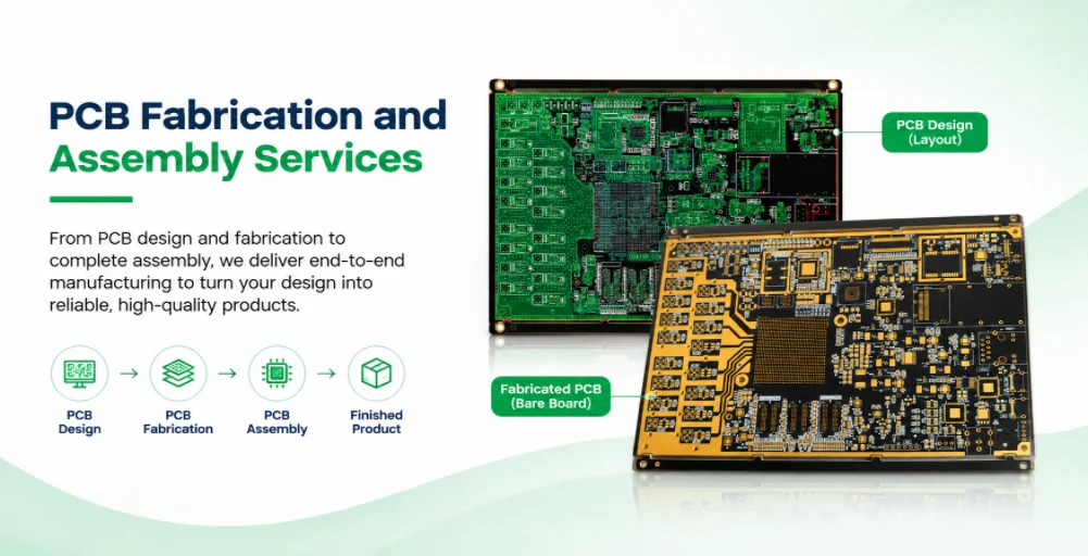
PCB Fabrication and Assembly Services
Highleap Electronics provides PCB fabrication and assembly...
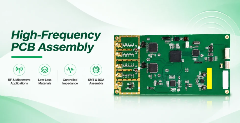
High Frequency PCB Assembly Services
Highleap Electronics provides high frequency PCB assembly...
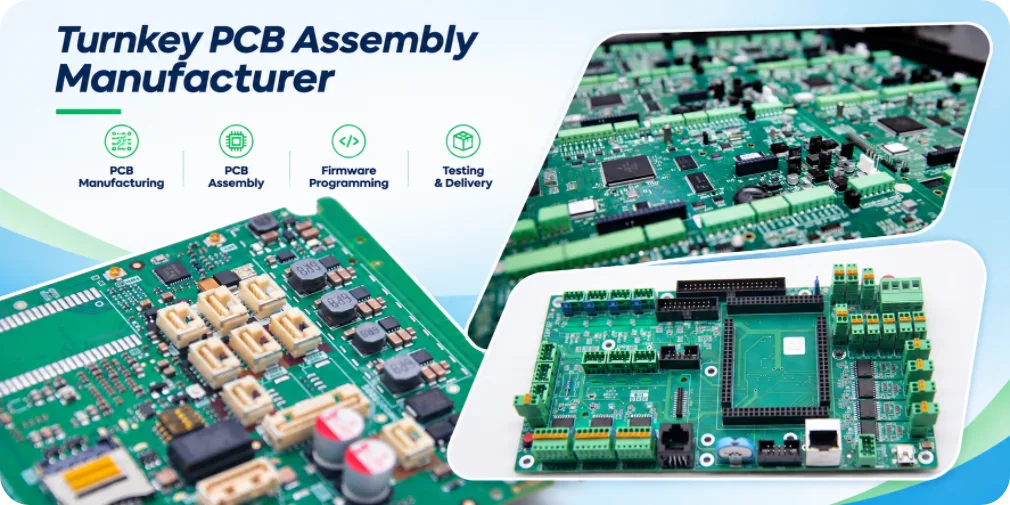
Turnkey PCB Assembly Manufacturer
Highleap Electronics is a turnkey PCB assembly...
How to get a quote for PCBs
Let‘s run DFM/DFA analysis for you and get back to you with a report. You can upload your files securely through our website. We require the following information in order to give you a quote:
-
- Gerber, ODB++, or .pcb, spec.
- BOM list if you require assembly
- Quantity
- Turn time
In addition to PCB manufacturing, we offer a comprehensive range of electronic services, including PCB design, PCBA, and turnkey solutions. Whether you need help with prototyping, design verification, component sourcing, or mass production, we provide end-to-end support to ensure your project’s success.
For PCBA services, please provide your BOM (Bill of Materials) and any specific assembly instructions. We also offer DFM/DFA analysis to optimize your designs for manufacturability and assembly, ensuring a smooth production process.