
PCB Fabrication Drawing Requirements for Special Processes
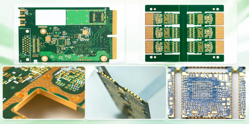
PCB fabrication drawings need to communicate more than board outlines and copper artwork when a design includes selective gold fingers, controlled-depth slots, milled cavities, edge plating, backdrilling or filled vias. Missing process details can delay quotation, trigger engineering questions or lead to manufacturing assumptions that affect fit and function. This guide explains which drawing callouts, supporting files and approval requirements buyers and engineers should prepare before releasing a special-process PCB for fabrication.
On This Page
Manufacturing feasibility and quotation scope depend on the supplied design and requirements.
PCB Fabrication Drawing Requirements for Special Processes
Gerber files describe copper artwork, solder mask and other defined image layers, while NC drill data communicates hole locations and drilling information. These files may not fully explain the intended manufacturing method, machining depth, localized plating, datum references or inspection criteria. A controlled fabrication drawing connects those requirements to specific features on the finished board.
For a PCB with special features, the manufacturing package should identify the board revision, finished dimensions, layer construction, material requirements, surface finishes, hole definitions and applicable acceptance criteria. Each critical feature should have a clear reference to its location and the relevant manufacturing instruction. If a drawing conflicts with the supplied Gerber, drill data or approved stackup, the discrepancy should be resolved before production release.
Board identification and dimensions
Part number, revision, units, finished outline, datum references, board thickness and dimensional tolerances.
Layer construction and materials
Laminate grade, approved substitutions, layer count, dielectric construction, copper requirements, solder mask and surface finish.
Special-process instructions
Localized plating, slot or cavity depth, via connections, fill and cap requirements, edge geometry and inspection details.
Acceptance and revision control
Applicable standard and revision, acceptance class where specified, electrical test, impedance requirements, inspection reports and change approvals.
A special-process drawing complements the broader PCB design-for-manufacturing checklist, which addresses other design and production-readiness considerations. The two serve different purposes: general DFM checks help identify manufacturability concerns, while detailed fabrication callouts define what the factory is expected to build and verify.
The required level of detail depends on the design. A conventional multilayer board may need only a standard fabrication package and clearly defined specifications. A board with blind slots, localized contact plating or controlled-depth milling usually needs additional views, dimensions and process-specific instructions.
Special PCB Processes and Required Drawing Callouts
The following matrix summarizes the information commonly needed to assess special-process PCB fabrication. Use the rows that apply to the actual design. Numerical limits, materials, process availability and inspection methods must be established for the specific project rather than assumed from a generic example.
| Process or feature | Drawing and data requirements | Items to confirm before production |
|---|---|---|
| Selective hard-gold fingers | Identify the contact region, finger dimensions, plating specification and thickness, bevel angle and affected side. | Plating method, contact-area boundaries, bevel clearance and applicable acceptance criteria. |
| Mixed-length or segmented gold fingers | Dimension finger lengths and segments, mark plating boundaries and identify the mating connector interface. | Contact engagement, plating continuity, selective pattern requirements and dimensional tolerances. |
| Blind or controlled-depth slot | Specify slot geometry, machining side, depth or remaining material thickness, tolerance and reference datum. | Tool access, residual laminate, depth measurement and inspection method. |
| Milled cavity or pocket | Define X-Y location and dimensions, depth or target floor thickness, datum and any restrictions on exposed copper. | Milling feasibility, remaining-layer clearance, local thickness and debris-control requirements. |
| Edge plating | Mark the metallized board edges, required finish, relevant dimensions and areas where plating must stop. | Plating and routing sequence, copper coverage, edge clearances and acceptance requirements. |
| Castellated holes | Identify half-hole locations, finished hole geometry, plating requirements and the final board edge. | Hole-to-edge registration, retained copper, fabrication sequence and inspection criteria. |
| Backdrilling | Specify entry side, drill diameter, target or stop layer, applicable net references and residual via-stub limit. | Layer depths, drill registration, remaining copper and the method used to verify the requirement. |
| Blind, buried and microvias | Identify connected layer pairs, drill and pad sizes, fill or cap requirements, and stacked or staggered via structure where applicable. | Sequential lamination requirements, registration, aspect-ratio constraints and reliability review. |
| Filled via-in-pad (VIPPO) | Identify via locations, fill material or process, copper capping, planarity and solderable finish requirements. | Approved filling process, cap construction, surface condition and acceptance criteria. |
| Press-fit connector holes | Define finished hole diameter and tolerance, plating requirements, insertion zone and connector part number. | Hole-size capability, component specification, finish compatibility and insertion-validation responsibility. |
| High-copper-weight construction | Specify finished copper weight or thickness by layer, where relevant, together with current-carrying and thermal design requirements. | Etching compensation, plating build, clearance requirements and manufacturing feasibility. |
| Fine-line and fine-space features | Identify minimum line/space requirements, critical clearances, affected layers and any controlled geometry. | Imaging and etching capability, copper thickness, compensation and yield considerations. |
| Multiple surface finishes | Map each finish to its designated area, specify the finish requirements and clearly define masking or boundary conditions. | Process-sequence compatibility, boundary control and suitability for the intended contacts or assembly process. |
| Controlled-impedance coupons and testing | Specify reference nets or layers, single-ended or differential targets, tolerance and required test reports. | Proposed stackup, trace geometry, coupon design and the agreed measurement and acceptance method. |
Important distinction for mechanical features
A blind slot, a milled pocket and a non-plated through slot describe different requirements. Identify the feature type explicitly and use a sectional view with a clear depth reference whenever the cut does not pass through the full board thickness. A note that only identifies a slot outline is insufficient if the intended depth remains undefined.
For selective contact finishes, the drawing should distinguish hard-gold contact areas from other finished copper surfaces. A general surface-finish note does not necessarily define the required localized plating, thickness or bevel. Similarly, backdrilling requires a clear reference to the entry side and target layer rather than a generic instruction to remove unused via barrels.
Do not assume that every advanced feature can be manufactured using the same process sequence. Confirm the proposed construction and acceptance method with the PCB manufacturer, particularly when several special processes interact in one design.
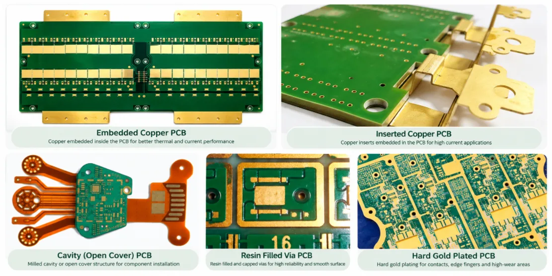
Common PCB Drawing Conflicts and Pre-Release Checks
Manufacturing delays often start with conflicting instructions rather than missing artwork. The following issues are worth resolving before sending the fabrication package for quotation or production release.
Slot geometry is shown, but depth is missing
The manufacturer cannot determine whether the feature is through-cut or blind. Add the machining side, depth reference, tolerance and a sectional view where needed.
Hard gold and general surface finish are confused
A drawing may specify hard gold while the finish note applies ENIG to the board generally. Mark the contact region and state the applicable finish requirements separately.
Stackup and fabrication files use inconsistent layer names
A net, reference plane or via connection may be interpreted against the wrong copper layer. Align layer naming across the stackup, artwork, drill tables and drawing.
Tolerance is specified without an unambiguous datum
A depth or profile requirement may be difficult to measure consistently without a defined reference. Identify the datum and the intended measurement method.
Example Fabrication Notes for Engineering Review
The following examples illustrate how to express manufacturing intent. Replace every placeholder with an approved project value, and confirm that the selected process can meet the specified requirements before releasing the drawing.
Illustrative callouts — not universal manufacturing specifications
1. Controlled-depth slot: ROUTE FROM [SIDE]; TARGET DEPTH [VALUE] ± [TOLERANCE], REFERENCED TO [DATUM SURFACE]; REMAINING MATERIAL THICKNESS [VALUE]. SEE SECTION [REFERENCE].
2. Gold fingers: APPLY [APPROVED CONTACT FINISH] TO THE IDENTIFIED CONTACT REGION ONLY; PLATING THICKNESS [SPECIFICATION]; BEVEL [ANGLE] ± [TOLERANCE], WHERE APPLICABLE.
3. Filled vias: VIA GROUP [REFERENCE] TO USE [APPROVED FILL AND CAPPING PROCESS]; PLANARITY AND ACCEPTANCE REQUIREMENTS PER [APPROVED SPECIFICATION].
4. Backdrilling: ENTRY SIDE [SIDE]; TARGET/STOP LAYER [LAYER]; MAXIMUM RESIDUAL STUB [VALUE]; VERIFICATION METHOD [METHOD].
5. Engineering changes: ANY PROPOSED DEVIATION AFFECTING MATERIAL, STACKUP, GEOMETRY OR A CRITICAL PROCESS REQUIRES CUSTOMER APPROVAL BEFORE IMPLEMENTATION.
All dimensions, tolerances, materials and acceptance criteria must come from the approved project specification and confirmed manufacturing process. The examples above are drafting references only; they should not be interpreted as standard limits for every PCB design.
Pre-Release Fabrication Drawing Checklist
- The part number and revision match the Gerber or ODB++ data, NC drill files and mechanical drawing.
- Every special feature has a defined location, geometry, process requirement and applicable tolerance or acceptance criterion.
- Controlled-depth features identify the machining side, datum and depth or remaining-thickness requirement.
- Plated and non-plated holes or slots are clearly distinguished, including edge plating and castellated features.
- Localized finishes are mapped to their intended areas, and hard-gold contacts are distinguished from general surface finishes.
- Layer count, stackup, via spans, impedance requirements and drill tables use consistent layer definitions.
- Required material certificates, cross-sections, impedance reports and acceptance standards are identified where applicable.
- Approval requirements are defined for material substitutions, stackup changes and critical process deviations.
- The approved drawing and fabrication data carry consistent revisions, and PCBA projects include the required BOM and assembly files.
Release the fabrication drawing as a controlled document within the manufacturing data package. Purchasing, engineering and manufacturing should work from the same approved revision. A concise drawing that resolves critical manufacturing decisions is more useful than a long document that leaves essential requirements open to interpretation.
PCB Fabrication and Assembly Engineering Review
A complete manufacturing package should reflect the actual PCB construction and any downstream assembly requirements. Layer count alone does not determine whether a board is HDI, and not every six-layer PCB requires microvias or sequential lamination. The necessary documentation depends on the selected construction, electrical constraints and special processes.
Layer Stackup and HDI-Specific Requirements
For a multilayer or HDI board, define the copper-layer sequence, dielectric construction, finished thickness and via connections clearly. If the design uses blind or buried vias, identify the connected layer pairs rather than relying on a generic via label. Designs involving sequential lamination should also identify the intended build-up structure and the requirements that need approval.
Controlled-impedance designs need a consistent relationship between the specified impedance, trace geometry, reference plane, dielectric construction and copper thickness. State the target and tolerance, identify the affected nets or layers, and indicate whether impedance coupons and measurement reports are required. The electrical requirement should remain explicit while the proposed manufacturable stackup is reviewed and approved.
For projects using six copper layers, the six-layer stackup and impedance-control relationship is relevant when checking whether the approved construction agrees with the fabrication data. For broader procurement planning, six-layer PCB fabrication and assembly requirements provide the appropriate context for the complete board order. These are related but distinct considerations: one concerns layer construction, while the other concerns the wider manufacturing and assembly project.
What Assembly Information Belongs in the Manufacturing Package?
If the purchase includes PCB assembly, fabrication drawings alone do not define the complete PCBA. Fine-pitch BGAs, press-fit connectors, castellated interfaces and special contact areas may require assembly views, component specifications or additional handling instructions. The fabrication and assembly data should be coordinated without assuming that one document replaces the other.
Prepare the BOM, pick-and-place or centroid data, assembly drawing and relevant revision information alongside the fabrication files. The BOM and placement data needed for PCBA help define the information required for assembly preparation. If a connector or component imposes specific board-interface requirements, ensure that the mechanical and assembly documentation agree.
Frequently Asked Questions About PCB Fabrication Drawings
Can Gerber files alone specify gold-finger plating?
Gerber artwork can identify the contact geometry, but it may not define the full plating specification, thickness, bevel or acceptance requirements. Provide a clear contact-region drawing and explicit finish notes that agree with the approved manufacturing specification.
How should a blind cavity or controlled-depth slot be dimensioned?
Show the feature location and geometry, machining side, datum, depth or remaining material thickness, tolerance and any critical layer-clearance requirement. A sectional view is useful when the cut depth cannot be understood from the plan view alone. Confirm the measurement method with the manufacturer.
Does every six-layer PCB need a special-process drawing?
No. A conventional six-layer board may be adequately defined by a standard fabrication package and approved specifications. Additional special-process callouts are necessary when ordinary layer artwork, drill data and standard notes do not fully communicate the required construction or acceptance conditions.
What should happen if the drawing and Gerber files conflict?
Resolve the discrepancy before manufacturing release rather than leaving the factory to choose which instruction to follow. A project-specific DFM review before production release can help identify manufacturability questions and document issues that need clarification. Any change affecting the approved design should follow the customer’s change-control process.
Request a PCB Fabrication or PCBA Quote
Share the approved drawing revision, fabrication data, layer stackup, order quantity and special-process requirements. If you also need assembly, include the BOM and placement files so the project scope can be evaluated together.

Recommended Posts

5G Small Cell PCB Manufacturing for RF and Telecom Infrastructure
Table of Contents 5G Small Cell PCB Requirements Depend on...
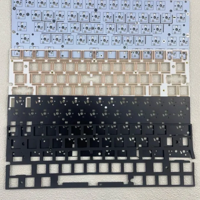
Custom 65% Keyboard PCB and PCBA Manufacturing
Table of contents 1. From Design Files to Production-Ready...
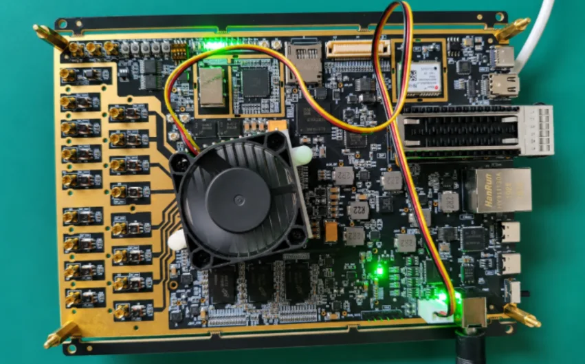
RFSoC Board PCB Manufacturing and Assembly One-Stop Service
Table of contentsReference RFSOC Board Project: 115 × 175...

How to Reduce PCB Costs in 2026
Table of contents Why 80% of PCB Cost Is Locked in at...
How to get a quote for PCBs
Let’s run DFM/DFA analysis for you and get back to you with a report. You can upload your files securely through our website. We require the following information in order to give you a quote:
-
- Gerber, ODB++, or .pcb, spec.
- BOM list if you require assembly
- Quantity
- Turn time
For PCBA services, please provide your BOM (Bill of Materials) and any specific assembly instructions. We also offer DFM/DFA analysis to optimize your designs for manufacturability and assembly, ensuring a smooth production process.