
PCB Resin Content: Stackup, Lamination and Manufacturing Guide
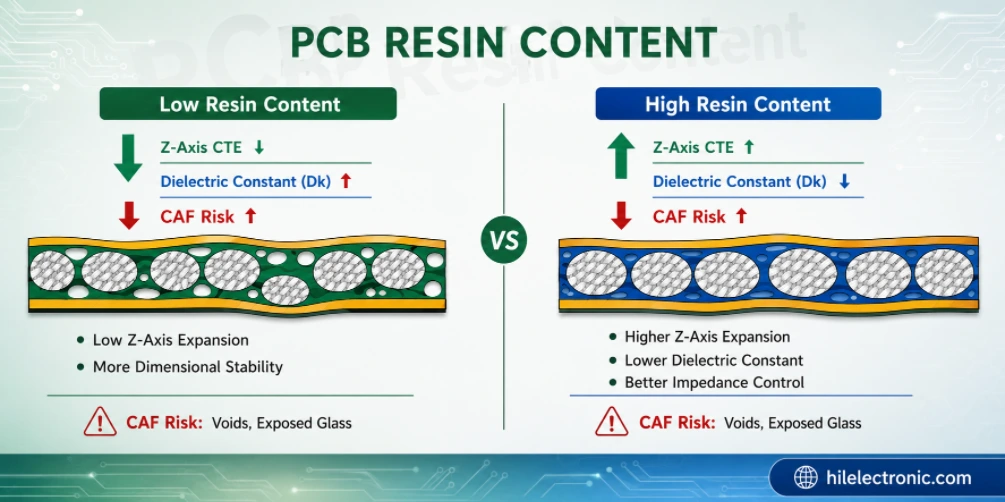
PCB resin content is the proportion of resin in a laminate or prepreg construction, commonly stated as a percentage by weight. It affects dielectric properties, pressed thickness, resin flow, copper fill, dimensional movement and multilayer reliability.
Highleap Electronics does not manufacture resin or prepreg. We select and process customer-approved material constructions, laminate the PCB, assemble the PCBA and verify the released requirements.
Why does PCB resin content matter? Because the same glass style with a different resin content can produce a different Dk, Df, pressed thickness and fill behavior. Quoting only the material family and glass style is insufficient for a controlled multilayer stackup.
What PCB Resin Content Means
Prepreg is partially cured resin carried by woven glass. During lamination, heat and pressure cause the resin to flow, fill copper topography and cure into the dielectric bond layer. Resin content influences how much material is available to fill spaces and how much glass remains in the final dielectric.
Higher resin content
More resin available for copper fill and potentially lower effective Dk, but greater flow, thickness variation or squeeze-out may occur.
Lower resin content
More glass fraction, often higher effective Dk and better dimensional stiffness, but reduced fill margin for heavy copper or open areas.
These are tendencies, not universal guarantees. Resin chemistry, glass style, cure cycle, copper pattern and pressure all interact.
This is not a stand-alone material or interface decision. The final behavior is produced by the interaction of resin flow during pressing with finished dielectric thickness and void control, while resin percentage and glass style and copper-area distribution determine whether the same design can be repeated across panels and material lots. That is why Highleap begins with the board files instead of a generic product questionnaire.
How Resin Content Affects Electrical and Mechanical Performance
| Area | Resin-content influence | Production consequence |
|---|---|---|
| Effective Dk | Glass and resin have different dielectric constants | Impedance geometry can change |
| Df | Resin and glass have different loss characteristics | Channel loss can change by construction |
| Pressed thickness | Available resin and copper distribution determine flow | Final dielectric spacing may differ from nominal |
| Resin fill | Must fill copper features and plane clearances | Risk of voids, starvation or poor bonding |
| Dimensional movement | Glass/resin ratio affects expansion and shrinkage | Registration and warpage |
| CAF and reliability | Resin, glass interface, drilling and moisture interact | Long-term insulation risk |
Repeatability is the main manufacturing test. A prototype can work even when the process window is broad, but volume production exposes variation in material lots, copper distribution, panel loading and plating. We place press-cycle and layup control, coupon and microsection review, stackup adjustment after DFM and prepreg construction selection in the production release to provide a stable comparison between lots.
Higher resin content generally means a larger resin-rich fraction after pressing, but the finished result also depends on glass style, copper coverage and resin flow. The change can influence effective Dk, dielectric thickness, dimensional movement, thermal expansion and the ability to fill around copper features. Highleap evaluates resin content as part of the stackup construction, not as an isolated percentage copied from a prepreg table.
How Resin Content Is Selected for a Stackup
- Review copper distribution: solid planes, dense signal layers and large clear areas demand different resin volumes.
- Check copper weight: heavier copper requires more fill.
- Set target pressed thickness: the dielectric thickness is a lamination result, not the uncured sheet thickness.
- Confirm impedance: Dk and final thickness must match the field-solver stackup.
- Balance the panel: asymmetric resin and copper can increase bow and twist.
- Qualify sequential lamination: each cycle changes thermal history and dimensional movement.
Generic datasheet values are not enough when ordinary electrical testing cannot detect impedance shift and plated-hole stress or resin starvation. The review must use the exact core or prepreg, copper profile, finished thickness and via route. This is where one-to-one engineering support prevents the buyer from having to interpret multiple supplier documents alone.
The output of the review should be a buildable stackup and a short list of controlled variables. Highleap documents the agreed material identity, geometry, process route and inspection basis, then coordinates the remaining details internally across CAM, fabrication, quality and assembly.
Implications of Using the Wrong Resin Content
- Resin starvation: insufficient resin leaves poor fill, weak bonding or exposed glass.
- Excessive squeeze-out: too much flow can reduce local dielectric thickness and create edge resin loss.
- Impedance shift: changed Dk and pressed thickness move the transmission-line geometry.
- Voids: trapped air or incomplete fill reduces reliability.
- Warpage: uneven resin and copper distribution creates stress.
- Registration error: dimensional movement can misalign fine features and vias.
These risks should lower the effort required to contact the factory, not raise it. Once Highleap receives the Gerber or design files, we check stackup adjustment after DFM, prepreg construction selection, press-cycle and layup control and coupon and microsection review. Only decisions that materially affect function, compliance, price or delivery are returned to the customer.
The purpose of describing these consequences is not to imply that every project will fail. It is to show which variables deserve review before purchase. The assigned engineer explains the specific exposure for the submitted design and coordinates any required change with fabrication, quality and assembly teams.
Prepreg Glass Style, Resin Content and Pressed Thickness
A prepreg designation is not complete without the construction and resin content. For example, two 1080-style prepregs can have different resin percentages and produce different electrical and flow behavior.
Highleap uses supplier construction data and internal process experience to propose a press package, then confirms the finished stackup through thickness measurement, cross-section and impedance correlation where required.
Design intent and factory compensation have different owners. The customer defines electrical and reliability requirements; Highleap applies the approved CAM, drilling, plating and lamination adjustments needed to reach the finished values. Any change that affects architecture or qualification is raised for approval instead of being hidden inside CAM processing.
Repeatability is the main manufacturing test. A prototype can work even when the process window is broad, but volume production exposes variation in material lots, copper distribution, panel loading and plating. We place prepreg construction selection, press-cycle and layup control, coupon and microsection review and stackup adjustment after DFM in the production release to provide a stable comparison between lots.
Resin Content in High-Speed and RF PCBs
At high speed, resin content changes the effective dielectric mix and can affect glass-weave behavior, skew and loss. A channel model that uses a single bulk Dk for every layer can miss construction-specific differences.
For RF and mmWave structures, resin flow and final thickness can directly shift impedance and resonant frequency. Tight control may require specified core constructions rather than prepreg-defined critical dielectric layers.
The technical variables in this section cannot be evaluated independently. A change in copper-area distribution can alter the effect of resin flow during pressing, while finished dielectric thickness and void control and resin percentage and glass style influence the geometry and test result seen on the finished board. Highleap reviews the actual production construction so the stackup and compensation are based on purchasable materials rather than nominal examples.
For controlled-impedance and low-loss layers, the pressed dielectric thickness and resin/glass distribution must match the field-solver assumptions. A resin-rich construction can reduce local glass influence but may increase thickness variation or movement if the copper pattern and press cycle are not balanced. RF and high-speed projects therefore require the exact prepreg construction, not only a nominal finished board thickness.
Highleap Multilayer Lamination Controls
- material and prepreg construction verification;
- copper-density and resin-demand review;
- vacuum lamination with controlled heat, pressure and cure;
- panel scaling and registration compensation;
- final thickness and bow/twist inspection;
- microsection for dielectric, plating and void evaluation;
- impedance coupon correlation;
- material lot and process traceability when required.
A capability claim has value only when it is connected to a controlled shop-floor route. Highleap links prepreg construction selection, press-cycle and layup control, coupon and microsection review and stackup adjustment after DFM to incoming inspection, lamination, drilling, plating, imaging and final verification. The exact sequence remains subject to the approved material and board construction.
Different designs require different process windows. Board thickness, material chemistry, copper balance, hole architecture and panel size can change preparation, pressing and plating conditions. The assigned engineer coordinates CAM, production and quality so the customer receives one manufacturing answer instead of separate questions from each department.
Why Resin Content Still Matters After Fabrication
The cured dielectric affects board stiffness, moisture response, Z-axis expansion and reflow behavior. High-density assemblies, large BGAs and repeated thermal cycles can expose weak lamination or warpage. Highleap reviews the bare-board construction and assembly profile together.
A capability claim has value only when it is connected to a controlled shop-floor route. Highleap links press-cycle and layup control, coupon and microsection review, stackup adjustment after DFM and prepreg construction selection to incoming inspection, lamination, drilling, plating, imaging and final verification. The exact sequence remains subject to the approved material and board construction.
The lamination result affects later operations. Resin starvation or voids can weaken interlayer bonding and expose hole walls to reliability problems, while excessive resin flow can shift thickness, registration and board flatness. During assembly, moisture absorption and repeated thermal cycles act on the cured resin system. Microsection and thickness data provide evidence that the intended construction was actually achieved.
Send the Gerber or PCB Design Files for Stackup Review
You do not need to calculate resin content before asking Highleap for a quotation. Send the Gerber files or native PCB design files first. If the stackup and fabrication notes are already included, they can be reviewed directly without a separate form.
Our lamination engineers complete the production discussion
Your Highleap engineer will review copper distribution, layer structure, target thickness and impedance with our stackup and lamination team. We will identify the suitable prepreg construction and contact you one to one only when a design choice or customer approval is needed.
Incomplete early data does not automatically stop the quotation. We identify what is already defined, distinguish preferences from mandatory requirements, and explain which unresolved decision is genuinely blocking. If assembly is required, BOM and placement files can be supplied after the bare-board scope is understood.
Cost and Lead-Time Effects
Special resin-content constructions, multiple prepreg plies, controlled glass styles and sequential lamination can increase material cost and press complexity. However, an under-filled or unstable construction creates much larger costs through scrap, requalification and field failures.
Lead time is often controlled by material availability, special copper, supplier minimums, sequential processing or outside characterization. The engineer identifies the actual schedule constraint and checks whether an approved alternative can remove it without changing the product requirement.
Yield must be considered from prototype through volume. Features associated with impedance shift and plated-hole stress or excessive thickness variation can increase scrap, rework and component loss. A stable documented construction usually has a lower total cost than an aggressive design that needs repeated changes after assembly.
A difficult resin-fill condition may require a different prepreg, additional plies, copper thieving, revised layer copper balance or a modified press cycle. These changes affect material usage, engineering time and yield. Highleap can often reduce cost by correcting local copper-distribution problems rather than simply adding more resin or increasing the total board thickness.
Resin Content Is a Production Variable, Not a Datasheet Footnote
Resin content links material selection to lamination, electrical performance and reliability. Highleap controls the approved construction and verifies the final board instead of treating all prepregs with the same glass style as interchangeable.
The percentage printed in a prepreg table does not directly state the final bond-line thickness or resin distribution in the PCB. Those results are created during lamination by the selected glass style, copper pattern, pressure, temperature and vacuum cycle. Highleap turns the design into a manufacturable layup and verifies the result through controlled pressing, thickness measurement and microsection where required.
For an initial review, the buyer only needs to send the Gerber or PCB design files. Our stackup and lamination engineers can identify whether the copper pattern creates unusual resin demand and then discuss any required construction change one to one. The customer does not need to calculate resin percentage before requesting a quotation.
Frequently Asked Questions
Is resin content the same as resin flow?
No. Resin content is the amount of resin in the construction; flow describes how it moves under a defined lamination test or process.
Does higher resin content always mean lower Dk?
Often the effective Dk decreases as resin fraction increases because E-glass usually has higher Dk, but the exact result depends on the resin system and construction.
Can two prepregs with the same glass style be substituted?
Not automatically. Resin content, resin chemistry, flow, cured thickness and electrical properties may differ.
How is pressed thickness controlled?
By selecting the construction and ply count, analyzing copper demand, and controlling lamination temperature, pressure, vacuum and cure.
Does Highleap manufacture prepreg?
No. We manufacture PCBs and PCBAs using approved laminate and prepreg from qualified suppliers.
Do I need to calculate resin content before requesting a PCB quote?
No. Send the Gerber files or native PCB design files first. Highleap will review the stackup and copper distribution with the lamination team and confirm any required prepreg or resin-content decisions with you.
Technical reference note: Material properties and interface descriptions must be checked against the current manufacturer datasheet, customer specification and applicable interface standard for the exact production construction. Highleap Electronics is the PCB fabrication and PCB assembly provider; laminate and component trademarks belong to their respective manufacturers.

Recommended Posts

Taconic RF 35 vs RO4350B PCB
Table of contentsRF-35 vs RO4350B Procurement and...

TMM4 Filter PCB Manufacturing
TMM4 filter PCB manufacturing is controlled by the...

TMM3 PCB Manufacturing for RF Modules
TMM3 PCB manufacturing is most useful where the RF module...

TMM6 PCB Fabrication
TMM6 fabrication is the process-control page for a mid-Dk...
How to get a quote for PCBs
Let’s run DFM/DFA analysis for you and get back to you with a report. You can upload your files securely through our website. We require the following information in order to give you a quote:
-
- Gerber, ODB++, or .pcb, spec.
- BOM list if you require assembly
- Quantity
- Turn time
For PCBA services, please provide your BOM (Bill of Materials) and any specific assembly instructions. We also offer DFM/DFA analysis to optimize your designs for manufacturability and assembly, ensuring a smooth production process.