
Lead Free PCB Material for PCB Assembly and Reliable PCBA Manufacturing
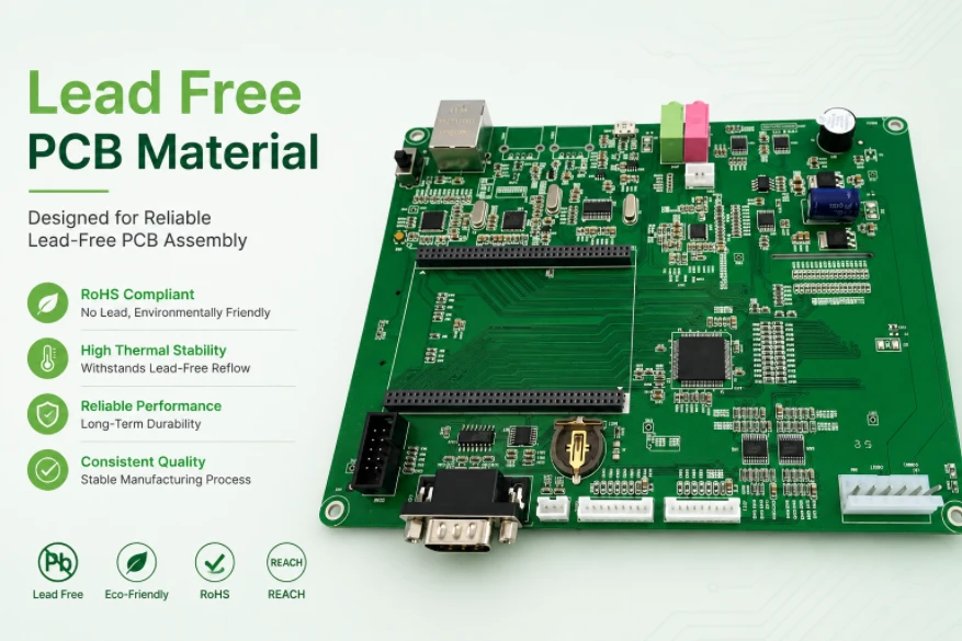
Lead free PCB material selection belongs in the assembly discussion, not only in the bare-board specification. The practical question is whether the laminate, surface finish, solder mask, package mix, and reflow process can support a stable lead-free build without creating warpage, wetting, or inspection problems later in production.
Highleap Electronics reviews lead-free boards as complete PCBA projects. We connect laminate choice with lead-free PCB, lead-free solder, stencil design, SMT assembly, and inspection coverage so the board can move cleanly from fabrication to repeatable assembly.
What Lead-Free Material Selection Really Means
The goal is assembly reliability, not a label on the drawing
Many drawings mention lead-free compatibility without clarifying what problem must be solved. In practice, the material review is about whether the board can survive higher reflow temperatures, maintain flatness, support the chosen surface finish, and pass inspection after assembly.
That means the laminate discussion should be connected to the actual component set and process route. A board built with small passive parts and simple SMT may not need the same material decision as a dense BGA assembly or a multilayer industrial control board.
Lead-free requirements often come from the assembly floor
The strongest signals are usually practical ones: repeated reflow exposure, package sensitivity, warpage concerns, or export compliance expectations. Highleap therefore prefers to review material selection together with assembly files rather than as a disconnected bare-board topic.
How Reflow Stress Changes the PCB Decision
The reflow profile can expose weaknesses that do not appear in fabrication alone
Lead-free assembly typically brings higher process temperatures than tin-lead soldering, which can increase stress on the laminate, plated holes, solder mask, and larger package areas. If the board is thin, poorly balanced, or crowded with larger thermal masses, that stress becomes more important.
- Laminate thermal endurance and dimensional stability
- Board thickness and copper balance
- Expected number of reflow cycles and any rework exposure
- Large components or heat-sinking regions that change local thermal behavior
For this reason, a lead-free board review should include process assumptions, not just a compliance statement. Where needed, Highleap aligns the recommendation with High Tg FR4 PCB manufacturing or other material paths that better support the thermal load.
Board flatness affects yield long before a field failure appears
Assemblies with fine-pitch parts, BGAs, or large connectors can lose yield if the board moves too much during the thermal cycle. In those builds, material selection and board structure should be treated as assembly yield decisions, not only fabrication details.
Surface Finish Choices for Lead-Free Assembly
The finish must match the package mix and storage plan
Lead-free soldering performance depends heavily on the selected surface finish. ENIG, ENEPIG, OSP, immersion silver, immersion tin, and lead-free HASL each create different tradeoffs in flatness, storage life, cost, and assembly consistency.
| Finish | Typical fit | Common caution |
|---|---|---|
| ENIG / ENEPIG | Fine pitch, BGA, higher-value builds | Cost and process control |
| OSP | Cost-sensitive SMT with controlled storage | Shelf-life and handling sensitivity |
| Lead-free HASL | Boards where flatness is less critical | Planarity limits for fine pitch |
Highleap confirms the finish against the package mix and the storage or shipping expectation before finalizing the assembly route.
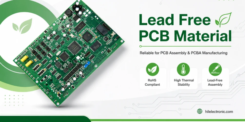
Package Mix, MSL, and Inspection Planning
Component sensitivity often defines the safe process window
Lead-free compatibility depends on the BOM as much as the board. Moisture-sensitive devices, large thermal pads, BGAs, QFNs, press-fit connectors, and mixed through-hole assemblies all change how the board should be built and inspected.
Highleap reviews MSL handling, baking requirements, stencil strategy, X-ray coverage, and any functional-test expectation before releasing the assembly plan. Related projects often overlap with PCB assembly services and higher-control builds where process discipline matters more than raw board price.
Inspection scope should match the actual assembly risk
A simple AOI-only flow may be enough for some SMT boards, but a denser lead-free build with BGAs or hidden joints can require X-ray or additional verification. The right inspection package should be set before the quote, not added after the line setup is already planned.
Where Fabrication and Assembly Need to Be Aligned
The fabrication notes should support the assembly process
Lead-free boards perform better when pad finish, solder mask definition, copper balance, and panel strategy are chosen with assembly in mind. If the bare-board files and the assembly files were prepared independently, Highleap checks for mismatch before production release.
This is especially important on boards with BGA escape routing, tight spacing, larger copper planes, or mixed SMT and through-hole content. In those cases, material choice, finish choice, and inspection planning should move together rather than in separate late-stage discussions.
Repeat production needs a locked process window
Once a lead-free assembly is validated, the material, finish, paste family, and inspection assumptions should be carried forward clearly. Otherwise the next order can reopen avoidable questions and create variation where the first build was stable.
What Highleap Needs for a Lead-Free PCBA Quote
A complete package allows a more accurate assembly response
- Gerber or ODB++, drill data, and fabrication notes
- BOM, pick-and-place, and assembly drawing
- Surface finish and any approved material requirements
- MSL or special handling notes for sensitive components
- Inspection scope such as AOI, X-ray, or functional test
- Target quantity, lead time, and compliance expectations
That information lets Highleap evaluate the lead-free board as a real PCBA program rather than as a partial documentation set.
FAQs
Does every lead-free build need High Tg material?
No. It depends on the board structure, the package mix, and the process exposure. Some assemblies work well on standard materials, while others benefit from a thermal upgrade.
Is ENIG always the best finish for lead-free assembly?
Not always. It is a strong option for many fine-pitch builds, but the best finish depends on flatness, cost, shelf life, and the component mix.
Can Highleap review both the bare board and the assembly package together?
Yes. That is usually the best way to avoid yield loss caused by a disconnect between fabrication assumptions and the real assembly process.

Recommended Posts

Taconic RF 35 vs RO4350B PCB
Table of contentsRF-35 vs RO4350B Procurement and...

TMM4 Filter PCB Manufacturing
TMM4 filter PCB manufacturing is controlled by the...

TMM3 PCB Manufacturing for RF Modules
TMM3 PCB manufacturing is most useful where the RF module...

TMM6 PCB Fabrication
TMM6 fabrication is the process-control page for a mid-Dk...
How to get a quote for PCBs
Let’s run DFM/DFA analysis for you and get back to you with a report. You can upload your files securely through our website. We require the following information in order to give you a quote:
-
- Gerber, ODB++, or .pcb, spec.
- BOM list if you require assembly
- Quantity
- Turn time
For PCBA services, please provide your BOM (Bill of Materials) and any specific assembly instructions. We also offer DFM/DFA analysis to optimize your designs for manufacturability and assembly, ensuring a smooth production process.