
RT duroid 6010.2LM PCB Manufacturing
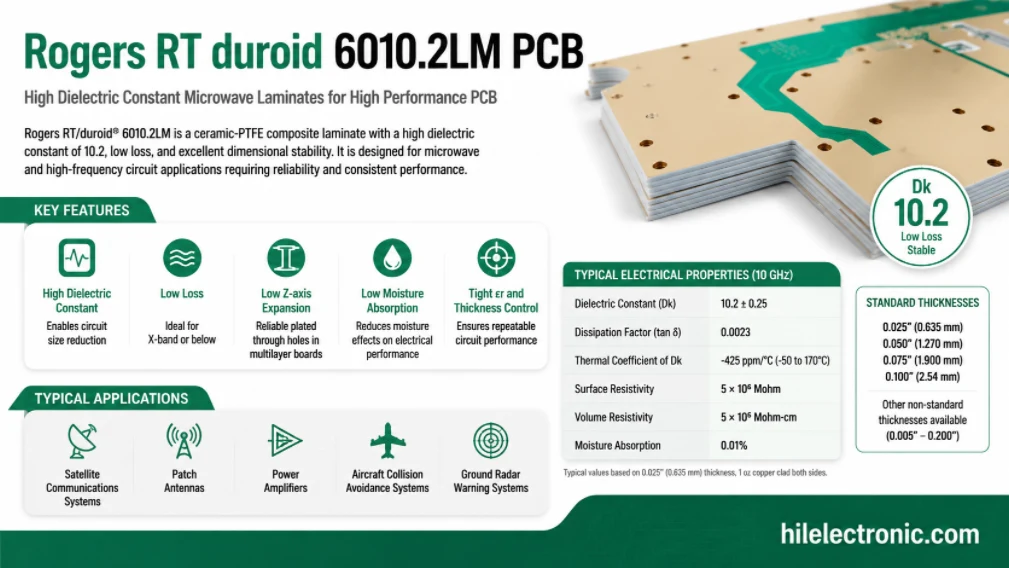
Highleap Electronics manufactures and assembles Rogers RT/duroid 6010.2LM PCBs for compact microwave circuits, filters, resonators, matching networks, radar modules, and other high-Dk RF designs. We support engineering review for prototypes, low-volume builds, and repeat production, with the exact capability confirmed from your stackup, geometry, hole structure, material construction, and test requirements.
The 6010.2LM page focuses on fabrication and production control for a high-Dk PTFE-based construction. Stackup definition, drilling, plated-hole preparation, dimensional checks and the transition from prototype to repeat production are the main manufacturing concerns.
RT/duroid 6010.2LM PCB Build Support
RT duroid 6010.2LM PCB manufacturing is suited to high-Dk RF structures where board area and electrical dimensions are closely linked. The production target is a stable finished geometry that matches the released RF model. Highleap can evaluate RT/duroid 6010.2LM multilayers, hybrid RF stackups, controlled-impedance transitions, plated vias, cavities, compact high-Dk circuit layouts, and advanced interconnect structures. For difficult builds, the review covers dielectric construction, copper treatment, drilling and plating route, lamination behavior, RF acceptance method, and assembly constraints before a manufacturing commitment is made. For tightly coupled RF features, high-Dk board fabrication planning should be completed before minimum line and gap tolerances are approved.
Important: Projects may be supplied as RF prototypes, qualification lots, or repeat production. The final route is tailored to the actual laminate, stackup, geometry, and test requirement rather than limited by a one-size-fits-all material capability statement.
Best fit
Compact microwave filters, resonators, couplers, matching circuits, power-amplifier networks, radar and aerospace RF modules.
Poor fit
Ordinary digital boards, cost-driven FR-4 products, or antennas and wideband structures that benefit from lower dielectric loading.
Manufacturing scope
Material verification, stackup, controlled impedance, qualified PTFE processing, multilayer or hybrid fabrication, surface finish, assembly, inspection, and customer-defined test.
Send for quotation
Fabrication data, stackup, exact material and copper, impedance/RF criteria, dimensions, holes, quantity, delivery target, plus BOM and assembly files when PCBA is required.
Is RT/duroid 6010.2LM the Right Material for Your PCB?
RT/duroid 6010.2LM is a ceramic-filled PTFE laminate selected mainly for compact microwave structures. Rogers publishes a process dielectric constant of 10.2 ± 0.25, a design value of 10.7, and a typical dissipation factor of 0.0023 at 10 GHz. The high dielectric constant allows resonators, filters, couplers, matching networks, and other distributed circuits to occupy less area than equivalent structures on a low-Dk laminate.
Choose it when
- circuit miniaturization is a primary requirement;
- the RF model is already based on the approved 6010.2LM construction;
- narrow controlled-impedance lines and tight RF dimensions can be manufactured and inspected;
- the operating-temperature effect on phase or resonance has been considered.
Do not choose it automatically when
- the board is an ordinary digital or power PCB;
- the design needs the lowest possible transmission loss rather than compact size;
- the antenna benefits from lower dielectric loading and wider traces;
- the project has not fixed laminate thickness, copper type, or modelling basis.
The key commercial question is not whether Highleap has heard of the material. It is whether the submitted construction can be converted into a repeatable stackup, drilled and plated with a qualified PTFE process, assembled without disturbing RF-critical structures, and tested against criteria the customer actually accepts.
What Highleap Can Review and Manufacture
Highleap Electronics can review RT/duroid 6010.2LM projects for rigid RF boards, multilayer constructions, and hybrid Rogers/FR-4 stackups. A quotation may include bare-board fabrication only or a coordinated PCB assembly package. Final capability depends on the real layer count, overall thickness, hole structure, panel dimensions, critical line widths and gaps, copper weight, tolerances, and test plan.
| Project item | Highleap review scope | What the customer receives |
|---|---|---|
| Material and stackup | Confirm 6010.2LM grade, thickness, copper, bonding material, hybrid compatibility, symmetry, and current supply. | A proposed production stackup or a list of unresolved material decisions. |
| Controlled impedance | Model the agreed Dk basis, finished copper, dielectric thickness, etch compensation, solder mask, and coupon structure. | Manufacturing geometry for approval and an impedance-test plan where specified. |
| PTFE fabrication | Review drilling, hole-wall activation, plasma or approved treatment, plating, registration, routing, and handling. | A qualified process route tied to the submitted design. |
| Surface finish and assembly | Check ENIG, immersion silver, or other specified finish against RF pads, connectors, soldering, storage, and cleaning. | A coordinated bare-board and PCBA release plan. |
| Inspection and test | Plan netlist test, critical-dimension inspection, microsection, impedance or resonator coupons, AOI, X-ray, functional or RF test. | Defined acceptance evidence rather than a generic “RF tested” statement. |
Prototype, low-volume, and volume production can be evaluated from the same controlled data package. A prototype that uses substitute material, simplified coupons, or relaxed geometry without written approval is not a valid path to mass production.
Design Information Required Before Tooling
A high-Dk design is sensitive to incomplete input. Sending only Gerber files and the phrase “Rogers 6010 PCB” leaves the factory to guess the most important electrical variables. The RFQ should identify the exact material construction and the basis used in the customer’s simulation. When comparing RO3210 as another high-permittivity construction, retain separate material properties and dimensional requirements for each proposed design.
Minimum fabrication package
- Gerber, ODB++, or IPC-2581 data and an IPC-356 netlist;
- fabrication drawing, readme, dimensions, tolerances, hole table, and panel requirements;
- complete layer stackup with 6010.2LM thickness, bonding material, copper foil, and finished copper;
- single-ended and differential impedance table, reference layers, tolerance, and coupon requirement;
- frequency range, RF-critical dimensions, phase, resonance, or insertion-loss acceptance criteria;
- surface finish, solder-mask treatment, via-fill requirement, and any controlled back drilling or cavity details;
- quantity, prototype/production forecast, delivery target, quality class, traceability, and certificate requirements.
Additional PCBA package
- BOM with approved manufacturer part numbers and substitutions policy;
- centroid/pick-and-place data, assembly drawing, polarity, and special handling notes;
- stencil or solder-volume requirements for launches, shields, and connectors;
- reflow, cleaning, conformal coating, functional test, RF test, and programming requirements.
Highleap can help refine the stackup and perform DFM, but the customer must approve any geometry, material, or acceptance change that can alter RF performance.
Material scope: Highleap Electronics is the PCB manufacturer and assembler for the build described here. Rogers and the referenced grade names identify the specified material and are not a description of Highleap material manufacturing.
How the PCB Is Fabricated
The manufacturing route is driven by PTFE chemistry and by the narrow geometry created by the high dielectric constant. A typical release includes the following controls:
- Material verification and conditioning. Incoming laminate identity, thickness, copper, lot traceability, and storage condition are checked before tooling.
- CAM and artwork compensation. RF-critical lines, gaps, pads, resonators, and registration targets are separated from ordinary dimensions. Compensation is based on copper weight and the qualified etch process.
- Drilling and hole preparation. Tooling, feeds, support materials, smear control, and PTFE activation are selected for the actual hole range and stackup.
- Copper deposition and plating. Hole-wall coverage, finished copper, annular rings, and RF ground-via structures are controlled without unnecessarily changing critical surface geometry.
- Multilayer bonding where applicable. The bonding film or prepreg, press cycle, resin fill, thickness, registration, and CTE interaction are qualified as a system.
- Patterning and finish. Etch compensation, line inspection, surface finish, solder-mask clearance, routing, and edge quality are checked against RF requirements.
- Final verification. Electrical test, dimensional inspection, microsection, impedance or RF coupon data, traceability, and customer-specific test evidence are compiled for release.
This process is the practical difference between a material reseller and a PCB manufacturer. Stock availability alone does not prove the ability to fabricate the requested structure.
Product-Level Build Trade-Offs
Microwave filters and resonators
The high Dk reduces physical resonator length and can help fit a compact filter into a constrained module. The trade-off is greater sensitivity to etched width, dielectric thickness, copper profile, RF surface finish, and temperature. The quotation should therefore include critical-dimension inspection and a clear frequency or coupon acceptance method.
Power amplifiers and matching networks
Compact matching structures and bias networks can benefit from the material, but thermal design must still use copper, thermal vias, heat spreaders, mounting, and airflow. The laminate should not be described as a complete thermal solution.
Radar, aerospace, and microwave communication
6010.2LM can support compact RF modules where space and repeatability matter. Environmental qualification, connector launches, housing interaction, phase stability, and assembly cleanliness must be defined at the product level.
When a lower-Dk material may be better
Antennas, wideband interconnects, and designs requiring wider, less etch-sensitive conductors may be better served by a lower-Dk laminate. Highleap can quote only after the customer identifies the electrical objective; “higher Dk” is not automatically “better RF performance.”
Cost, Lead Time, and Production Risk
There is no responsible fixed price per square metre for this material. The cost is created by the complete build and by the amount of engineering and inspection required to make it repeatable.
| Cost driver | Why it changes the quotation | How to control it |
|---|---|---|
| Material thickness and copper availability | Nonstandard constructions can require special procurement, minimum order quantities, or longer supplier lead time. | Allow approved purchasable constructions and forecast repeat demand. |
| Layer count and hybrid bonding | More press cycles, mixed CTE, resin fill, and registration control increase process risk. | Use the simplest stackup that meets electrical requirements. |
| Critical geometry and impedance tolerance | Narrow lines, small gaps, and tight coupons increase tooling, inspection, and yield pressure. | Separate genuinely RF-critical tolerances from ordinary dimensions. |
| Hole quantity and via architecture | Small holes, dense ground-via fences, filled vias, blind vias, and high aspect ratio add drilling and plating work. | Review via function and remove unnecessary complexity. |
| Surface finish and testing | Finish thickness, microsections, RF coupons, S-parameters, and customer fixtures add direct cost. | Define the minimum evidence needed for acceptance before quotation. |
| Quantity and release maturity | Prototype setup cost is distributed over fewer boards; unstable revisions create repeated tooling and material risk. | Freeze stackup and acceptance criteria before volume release. |
Lead time is confirmed only after material availability, CAM questions, tooling, inspection, assembly, and test requirements are known. A promised calendar number before reviewing these items is sales language, not production planning.
Why Use Highleap for a 6010.2LM Project?
Highleap’s role is to connect the material callout to a manufacturable and inspectable product. The service can include material verification, stackup engineering, controlled-impedance review, PTFE fabrication, hybrid lamination, component sourcing, SMT and through-hole assembly, AOI/X-ray, and customer-defined functional or RF testing. Highleap’s review covers stackup, registration, copper definition and hole technology before CAM. Where the design is especially compact, first-article inspection should concentrate on the dielectric and conductor dimensions that determine the RF result. Exact material property values should be checked against the current supplier documentation for the specified grade and construction.
The practical deliverable is not an article about Rogers material. It is a written production interpretation: which construction will be purchased, how the board will be built, what must be changed, which tolerances are feasible, what will be measured, what affects cost, and what remains the customer’s system-level validation responsibility.
For related engineering detail, see the high-Dk Rogers fabrication guide, RF impedance-control guide, and Rogers/FR-4 hybrid stackup guide.
Commercial FAQ
Can Highleap manufacture a multilayer RT/duroid 6010.2LM PCB?
Yes, suitable multilayer and hybrid projects can be reviewed for fabrication and assembly. The final route depends on the bonding system, material thickness, layer count, via architecture, panel size, tolerances, and acceptance tests.
Do you keep RT/duroid 6010.2LM available for the specified RFQ?
Material availability varies by thickness, copper, region, and quantity. Highleap verifies current stock or procurement status during quotation and does not treat a family name as proof that the exact construction is available.
Which dielectric constant should be used for impedance modelling?
Do not choose automatically. The designer and fabricator should agree on the modelling method and the value associated with the current Rogers data and the actual production construction. The released geometry and coupon must use the same basis.
Can Highleap provide PCB assembly and RF testing?
PCB assembly can be quoted from the BOM, component packages, stencil, connector, cleaning, and test requirements. RF testing is customer-defined: provide the fixture, calibration method, limits, and reference planes, or request a proposal for suitable coupon or functional testing.
What is needed for a firm price and lead time?
Provide the complete fabrication package, stackup, exact material and copper, impedance requirements, quantities, delivery target, and any assembly and test files. Without those inputs, only a budgetary discussion is possible. For a quote, provide the exact grade, construction, board thickness, copper, operating frequency, impedance requirements and quantity. Include assembly data when the 6010.2LM board will ship as a finished PCBA.

Recommended Posts

TMM4 Filter PCB Manufacturing
TMM4 filter PCB manufacturing is controlled by the...

TMM3 PCB Manufacturing for RF Modules
TMM3 PCB manufacturing is most useful where the RF module...

TMM6 PCB Fabrication
TMM6 fabrication is the process-control page for a mid-Dk...

TMM10 PCB Manufacturing for Compact RF Designs
Table of contentsHow TMM10 Shrinks RF StructuresTMM10 vs...
How to get a quote for PCBs
Let’s run DFM/DFA analysis for you and get back to you with a report. You can upload your files securely through our website. We require the following information in order to give you a quote:
-
- Gerber, ODB++, or .pcb, spec.
- BOM list if you require assembly
- Quantity
- Turn time
For PCBA services, please provide your BOM (Bill of Materials) and any specific assembly instructions. We also offer DFM/DFA analysis to optimize your designs for manufacturability and assembly, ensuring a smooth production process.