
Taconic RF-30 PCB Manufacturer for Antenna and Low-PIM Boards
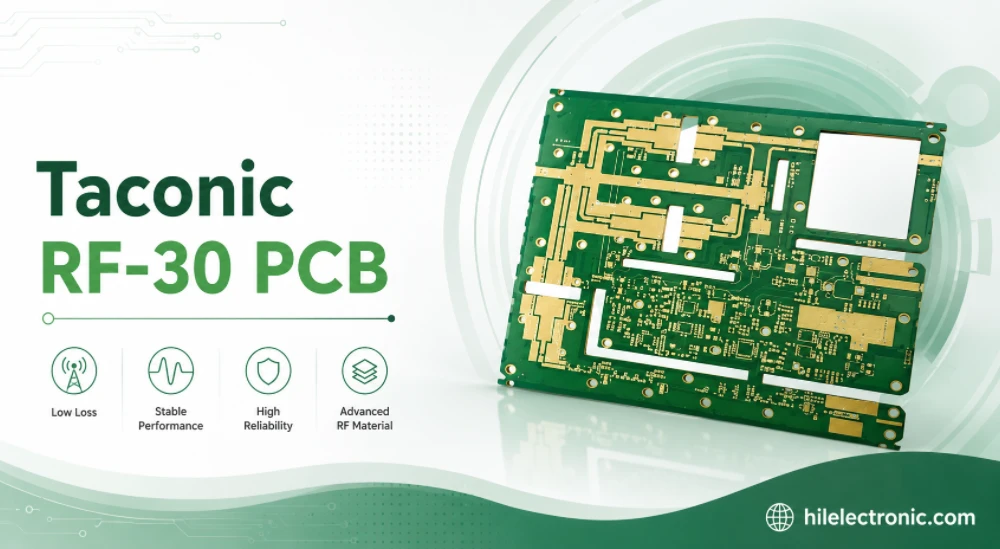
Highleap Electronics manufactures Taconic RF-30 PCB assemblies for base-station antennas, passive RF networks, filters, combiners, feed boards and communication modules. We support prototypes, pilot builds and repeat production with controlled RF geometry, large-panel handling, via-fence fabrication, connector assembly, low-PIM process controls and customer-defined testing.
RF-30 is a legacy designation, while RF-30A is the current AGC high-volume antenna material. Highleap verifies which grade is controlled by the drawing, confirms thickness, copper, certificate and substitution rules, and then issues a manufacturing route that protects existing antenna tuning and PIM requirements.
RF-30 and Current RF-30A Characteristics for Antenna Builds
Current AGC RF-30A is a woven-glass-reinforced, ceramic-filled PTFE laminate positioned for high-volume antennas and RF passive components. AGC lists Dk 2.97 ± 0.05 and Df 0.002, together with improved PIMD, PTH quality and mechanical stability. Legacy RF-30 must still be released against the customer’s controlled datasheet and cannot be renamed RF-30A without approval.
| Characteristic | Antenna-production benefit | Highleap control |
|---|---|---|
| Low-loss, approximately Dk-3 class | Supports antenna feed networks and passive RF structures with practical circuit dimensions. | Use the approved Dk model, finished dielectric and copper in geometry review. |
| Woven reinforcement in RF-30A | Supports mechanical stability for larger antenna panels and volume production. | Control panel orientation, imaging scale, registration and flatness. |
| PIM-oriented material positioning | Useful for base-station and passive networks where non-linear junctions must be controlled. | Define complete PIM interface, finish, connectors, cleaning and test method. |
| PTH and peel-strength benefits | Supports dense grounding and connector structures when processed correctly. | Release drilling, hole preparation, plating and microsection requirements. |
See the official AGC RF-30A product page. Highleap also links antenna manufacturability to its PCB antenna design guidance.
Taconic RF-30 PCB Manufacturing Capabilities
Highleap manufactures customer-specified RF-30 boards for base-station antennas, RF passive components, splitters, couplers, filters, feed networks, repeaters and related telecommunications assemblies. Projects may be two-layer microstrip circuits, plated-through-hole antenna boards, long-format panels or hybrid RF/control constructions, subject to factory DFM and material availability.
Highleap Support for Antenna and Passive RF Products
| Project area | Highleap project support |
|---|---|
| Board formats | Single/double-sided antenna circuits, PTH boards, arrays, feed networks and customer-approved multilayer hybrids |
| Panel handling | Large or elongated circuits with registration, flatness and handling plans matched to the product |
| Grounding | Dense via fences, connector grounds, mounting points and mechanical interfaces |
| Low-PIM controls | Material, copper, finish, cleanliness, connector torque/interface and test definition reviewed together |
| Assembly | RF connectors, cables, shields, passive components and mechanical hardware |
| Verification | Electrical test, dimensional inspection, agreed impedance/PIM evidence and customer-defined functional test |
Highleap Rigid RF PCB Manufacturing Capabilities
The figures below are Highleap’s published rigid-PCB factory limits. Large RF-30 antenna panels, dense ground-via patterns and low-PIM requirements can impose a narrower project-specific process window, which is confirmed during DFM. See the complete Highleap rigid PCB capability table for the published factory specification.
| Manufacturing item | Published Highleap capability | RF/PTFE project condition |
|---|---|---|
| Maximum layer count | Up to 60 layers | Layer count for a specific RF/PTFE or hybrid stackup is confirmed after lamination, registration, via and material review. |
| Minimum inner-layer trace/space | 2/2 mil (0.05/0.05 mm) | The released RF geometry also depends on copper thickness, foil type, etch compensation and critical-dimension tolerance. |
| Minimum outer-layer trace/space | 2/2 mil (0.05/0.05 mm) | Fine RF gaps and coupled structures require project-specific feasibility and inspection criteria. |
| Board thickness range | 0.2–8.0 mm | Available thickness for a named Taconic/AGC construction depends on laminate gauge, bonding method and approved stackup. |
| Board-thickness tolerance | ±0.1 mm below 1.0 mm; ±10% at 1.0 mm and above | RF connector launches and enclosure interfaces should state any tighter product-level requirement. |
| Minimum finished board size | 10 × 10 mm | Small circuits may require delivery in a manufacturing panel or array for fabrication and assembly. |
| Maximum finished board size | 22.5 × 47.5 in (571.5 × 1206.5 mm) | Large-format PTFE boards require separate review for material sheet size, registration, flatness, routing and shipment. |
| Minimum mechanical drill / annular ring | 0.15 mm / 0.127 mm | Final via design depends on board thickness, aspect ratio, plating requirement and material-specific drilling process. |
| Minimum laser drill / annular ring | 0.075 mm / 0.075 mm | Laser microvias are subject to dielectric thickness, capture-pad design, copper build and sequential-lamination review. |
| Mechanical-drill aspect ratio | Up to 20:1 | The achievable ratio for an RF/PTFE build must be confirmed with finished hole size, board thickness and plating requirement. |
| Laser-drill aspect ratio | 1:1 | Microvia geometry is released only after stackup and reliability review. |
| Maximum inner/outer copper | Up to 10 oz | Maximum copper cannot automatically be combined with the finest trace/space or every PTFE construction. |
| PTH / NPTH tolerance | PTH ±0.075 mm; NPTH ±0.05 mm | Connector and RF grounding holes should identify finished diameter and any tighter fit requirement. |
| Contour tolerance | ±0.1 mm | Edge launches, cavities, slots and connector locations may need a dedicated dimensional-control plan. |
| Controlled-impedance tolerance | Single-ended and differential: ±5 Ω at ≤50 Ω; ±7% above 50 Ω | The quoted tolerance applies to an approved stackup, coupon strategy and measurement method. |
| Available surface finishes | ENIG, ENEPIG, OSP, HASL, immersion silver, immersion tin, flash gold, hard gold and gold fingers | Finish selection is reviewed for RF loss, soldering, wire bonding, connector contact and environmental requirements. |
Capability-combination notice: values in the table are individual factory capability limits. Layer count, 2/2 mil geometry, 10 oz copper, maximum panel size, 20:1 aspect ratio and the thinnest board construction are not assumed to be simultaneously achievable. Highleap confirms the usable combination after reviewing the exact material, stackup, copper, drill, RF tolerance, surface finish and assembly package.
The current AGC portfolio lists RF-30A rather than legacy RF-30. Highleap therefore verifies whether the controlled drawing requires original RF-30, permits RF-30A, or allows another qualified material. The official AGC RF-30A page describes the current high-volume antenna material, while the AGC RF/microwave product table shows the active product family. No change is made without customer approval.
For manufacturing context, Highleap applies the process controls described in RF PCB manufacturing and returns a written stackup/material release before production.
Low-PIM Manufacturing Starts with the Complete Interface
RF-30 has historically been used in antenna and passive RF applications where passive intermodulation can be important. Low PIM is not created by laminate selection alone. Copper foil, surface condition, plated features, finish, contamination, connector design, solder joints, hardware pressure and the final test interface can all contribute.
| PIM source area | Production control | RFQ requirement |
|---|---|---|
| Copper and etched edges | Approved foil, controlled etch, clean handling and no damaged trace edges | Copper type/profile and critical conductor geometry. |
| Surface finish | Uniform, compatible finish with controlled process and storage | Specified finish and any PIM qualification history. |
| Plated holes and grounds | Consistent hole copper, clean ground interfaces and controlled via structure | Finished holes, copper and microsection requirement. |
| Connectors and hardware | Approved parts, clean mating surfaces, solder/torque control | Connector part number, installation method and torque. |
| Assembly residues | Controlled flux, cleaning and handling | Cleanliness standard and allowed chemistry. |
| PIM test | Defined frequencies, power, fixture, order and acceptance limit | Complete test method before quotation. |
Highleap aligns DFM and production with the principles in low-PIM PCB design and low-PIM material selection. A bare-board or assembled PIM guarantee is only issued against an agreed test method.
Large Antenna Panels, Registration, and Flatness
Antenna feed boards can be physically large, narrow, repetitive or mechanically referenced to housings and radiator structures. Highleap reviews panel size, copper balance, grain direction, tooling holes, fiducials, routing support and packaging before committing the route.
- critical radiator and feed-network dimensions are separated from nonfunctional outline tolerances;
- panel compensation accounts for material movement and copper distribution;
- registration between RF artwork, drilled grounds and mechanical datums is defined;
- flatness and twist requirements are matched to the assembly and enclosure interface;
- routing, V-scoring or tab routing is selected to control edge quality and handling;
- shipping support prevents bending, abrasion and connector damage.
Transmission-line dimensions are reviewed with the customer’s RF model and the design considerations in PCB antenna design and RF antenna structures. Highleap manufactures to the released geometry; it does not redesign the antenna pattern without an engineering change request.
RF-30 Material, Copper, and Surface-Finish Control
The material release identifies exact grade, dielectric thickness, copper weight/type, lot documentation and allowed alternatives. For legacy RF-30, Highleap confirms stock and certificates before price and date are final. If RF-30A or another material is proposed, the design owner must approve the new Dk/loss model, thickness and qualification plan.
RF-30 Material Availability and RF-30A Transition Control
Highleap can quote original RF-30 continuity, customer-supplied material or an approved RF-30A transition. The change is evaluated for Dk model, thickness, copper, antenna dimensions, PIM, PTH behaviour, certification and tuning. Production does not begin until the authorised route is documented.
Copper profile and finish influence conductor loss and PIM. Highleap reviews the options using high-frequency copper foil guidance and RF PCB surface-finish selection. The production traveler records the approved material and finish so repeat orders are not rebuilt from memory.
| Control record | Purpose |
|---|---|
| Incoming material identity and lot | Confirms grade, thickness, copper and certificate match the released order. |
| CAM compensation record | Preserves critical line and gap dimensions after etch. |
| First-article dimensional report | Verifies selected RF and mechanical features before full release. |
| Electrical and impedance results | Confirms continuity and specified transmission-line controls. |
| Assembly lot and connector traceability | Links components, soldering and hardware to the finished unit. |
| Nonconformance and corrective action | Provides containment, cause review and approved disposition. |
Antenna PCB Assembly and Production Testing
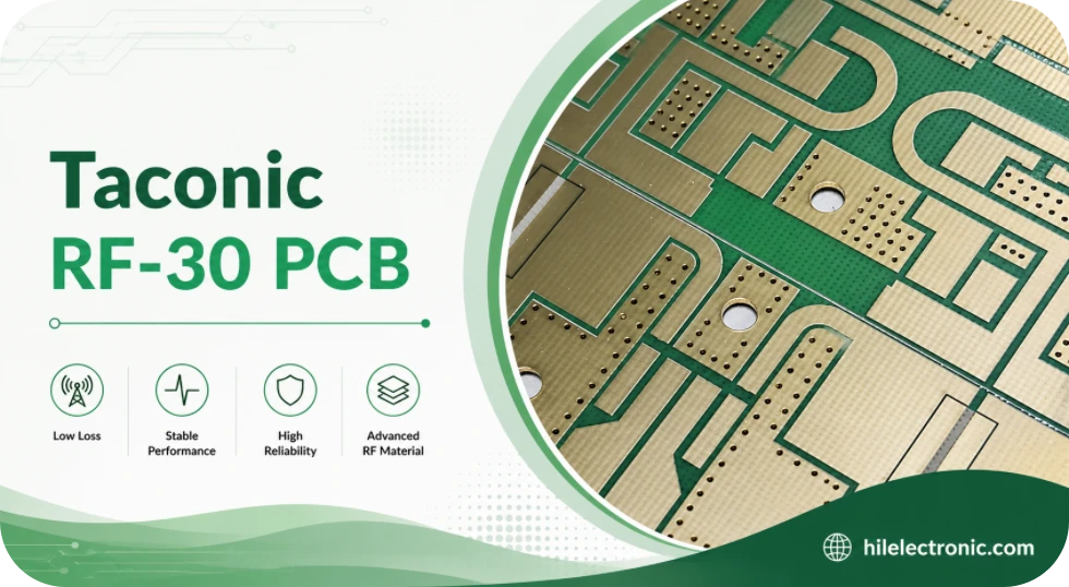
Highleap can deliver bare RF-30 antenna boards or complete assemblies with RF connectors, cables, shields, brackets, passives and control components. The assembly process follows the risks described in telecommunications PCB assembly and RF PCBA process control.
- BOM and connector verification against the released drawing;
- stencil/paste control for ground pads, shields and mixed thermal mass;
- fixture support to protect large or thin antenna circuits during soldering;
- controlled connector alignment and torque where specified;
- AOI, visual inspection and X-ray for hidden joints when applicable;
- continuity, DC function, RF or PIM testing according to the customer method;
- serialisation, test-data association and protective export packaging.
After shipment, Highleap supports record review, containment, failure-analysis coordination and corrective action. Repeat orders are controlled by approved revision, material route and test specification.
Lead Time and RF-30 Quotation Package
Highleap provides standard or expedited scheduling after material and panel-size feasibility are confirmed. The route may use priority fabrication, a first-article release or split shipment. See fast high-frequency PCB manufacturing for the scheduling approach.
For a complete PCB and PCBA route, Highleap can combine the RF laminate review with RF PCB assembly engineering and a formal production quotation.
After complete files are received, Highleap confirms material, panel utilisation, special tooling, connector availability and PIM/test readiness before fixing the quotation and shipment schedule. Large antenna panels and PIM fixtures are planned as explicit milestones rather than hidden assumptions.
Send Gerber/ODB++, controlled fabrication drawing, stackup, exact RF-30 or approved-alternative requirement, copper, critical RF dimensions, drill/route data, panel/flatness requirements, finish, quantities, delivery destination, BOM, assembly drawings and PIM/RF test method through Highleap Electronics. The broader Taconic material manufacturing page can be used when the grade is still under evaluation.
Can Highleap still make a Taconic RF-30 PCB?
Highleap can review legacy RF-30 production, but material availability, certificates and customer substitution rules must be confirmed before a firm commitment.
Can RF-30A be used instead of RF-30?
Only with written design-owner approval after electrical, mechanical, processing and qualification differences are reviewed.
Can Highleap guarantee low PIM?
A guarantee can only be tied to a defined material, assembly, fixture, frequency, power and acceptance method. Highleap can quote that controlled test route.
Can Highleap assemble large antenna boards?
Yes, subject to panel handling, fixture, flatness, connector and test review. These requirements should be included in the RFQ.
What information is required for an RF-30 antenna PCB quote?
Provide Gerber or ODB++, panel and mechanical drawings, material and copper specification, RF critical dimensions, PIM or impedance requirements, connector information, quantities, assembly files and delivery destination.
Does Highleap provide after-sales support for repeat antenna orders?
Yes. Highleap maintains revision, lot and process records, supports containment and corrective-action review, and controls approved material or process changes for subsequent builds.

Recommended Posts

Taconic RF 35 vs RO4350B PCB
Table of contentsRF-35 vs RO4350B Procurement and...

TMM4 Filter PCB Manufacturing
TMM4 filter PCB manufacturing is controlled by the...

TMM3 PCB Manufacturing for RF Modules
TMM3 PCB manufacturing is most useful where the RF module...

TMM6 PCB Fabrication
TMM6 fabrication is the process-control page for a mid-Dk...
How to get a quote for PCBs
Let’s run DFM/DFA analysis for you and get back to you with a report. You can upload your files securely through our website. We require the following information in order to give you a quote:
-
- Gerber, ODB++, or .pcb, spec.
- BOM list if you require assembly
- Quantity
- Turn time
For PCBA services, please provide your BOM (Bill of Materials) and any specific assembly instructions. We also offer DFM/DFA analysis to optimize your designs for manufacturability and assembly, ensuring a smooth production process.