
77 GHz Radar PCB Material Selection and Manufacturing Guide
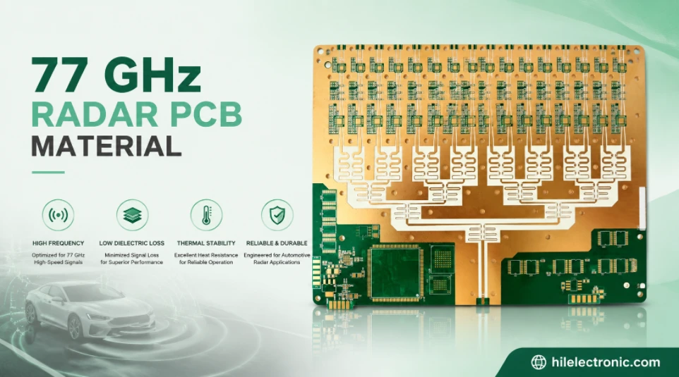
“77 GHz radar PCB material” is a selection problem, not a single product name. The correct laminate depends on antenna architecture, insertion loss, dielectric tolerance, temperature behavior, copper roughness, thickness, packaging and cost.
Highleap Electronics is a PCB manufacturer and PCB assembly factory. We do not manufacture laminate. We build radar PCBs using customer-approved materials from qualified suppliers and help convert the electrical design into a controlled fabrication and assembly release.
Which material should be used for a 77 GHz radar PCB? There is no universal answer. Ceramic-filled hydrocarbon, PTFE-based and other mmWave-capable laminates can work. The correct choice must be validated against antenna performance, loss, Dk stability, TCDk, copper profile, thickness tolerance, manufacturing route and qualification requirements.
What 77 GHz Changes in a PCB
At 77 GHz, the conductor pattern and local dielectric environment become part of the RF component. Small changes in line width, gap, dielectric thickness, copper roughness, solder mask or antenna geometry can shift impedance, phase and radiation behavior.
Loss
Dielectric loss and conductor loss both matter. Rough copper can erase the advantage of a low-Df resin.
Dimensional accuracy
Antenna patches, feed networks and transitions require controlled etch and final thickness.
Temperature stability
Automotive radar must remain predictable across a wide operating range.
Manufacturability
The material must support drilling, plating, multilayer bonding, assembly and volume yield.
When a risk remains, it is described in specific terms such as excess feed loss or phase imbalance across channels. This lets the customer approve a practical engineering choice instead of interpreting a long list of generic options.
At 77 GHz, dimensions that look small on an ordinary PCB become electrically significant. Etched line width, gap, copper thickness, dielectric thickness and the distance from an antenna feature to the board edge can shift impedance, phase and resonance. The antenna and feed network must therefore be treated as RF components, not simply as copper artwork. Highleap identifies the RF-critical dimensions separately from normal mechanical tolerances so inspection effort is applied where it affects performance.
The same sensitivity extends to production changes that would be minor on a lower-frequency board. A different copper foil, solder-mask opening, final board thickness or profile tolerance can alter the local electromagnetic environment. Highleap therefore separates RF-critical features from ordinary PCB dimensions and keeps the approved material construction and inspection basis under change control for repeat lots.
Common 77 GHz Radar PCB Material Families
| Material family | Potential advantage | Primary trade-off |
|---|---|---|
| Ceramic-filled hydrocarbon | Low loss, dimensional stability and practical multilayer processing | Exact Dk/Df and copper options vary by grade |
| PTFE-based laminate | Very low loss and mature microwave use | Processing, dimensional movement and bonding may be more demanding |
| Low-loss thermoset | Multilayer and HDI compatibility | Must be proven at the actual mmWave structure and loss target |
| Hybrid RF + FR-4 | Controls cost by placing premium material only where needed | Lamination compatibility, CTE and registration require qualification |
Examples of commercially available radar-capable materials exist from several suppliers, but similar published Dk values do not make them drop-in equivalents.
Generic datasheet values are not enough when ordinary electrical testing cannot detect connector or package transition mismatch or antenna resonance shift. The review must use the exact core or prepreg, copper profile, finished thickness and via route. This is where one-to-one engineering support prevents the buyer from having to interpret multiple supplier documents alone.
No material family is automatically correct for every radar board. PTFE-based laminates can provide low loss and stable RF behavior, while thermoset low-loss systems may offer easier multilayer processing and assembly. Hybrid constructions can combine an RF outer layer with conventional digital or power-control layers. The final choice depends on antenna architecture, operating temperature, layer count, board size, qualification history and available production constructions.
How to Select 77 GHz Radar PCB Material
- Start with the RF structure: antenna-in-package, antenna-on-PCB, microstrip, stripline or waveguide transition.
- Define the loss budget: separate dielectric, copper, launch, via and radiation losses.
- Specify Dk correctly: use the supplier’s relevant design value and the agreed field-solver method.
- Control copper profile: select an approved low-profile foil and include it in the model.
- Check temperature behavior: review Dk stability, CTE, moisture and operating range.
- Confirm available thicknesses: the model must use a purchasable production construction.
- Qualify the manufacturing route: drilling, plating, hybrid lamination, solder mask and finish.
Design intent and factory compensation have different owners. The customer defines electrical and reliability requirements; Highleap applies the approved CAM, drilling, plating and lamination adjustments needed to reach the finished values. Any change that affects architecture or qualification is raised for approval instead of being hidden inside CAM processing.
The selection should be tested against the full radar structure. Dk stability influences antenna and feed dimensions; Df and copper roughness affect loss; thickness tolerance changes impedance and resonance; CTE and reinforcement influence registration and environmental stability. Highleap can review the requested material against these production variables, but the customer retains approval of the RF model and any proposed equivalent.
Implications of Choosing the Wrong Radar Material
- Antenna resonance or beam characteristics can shift because of Dk or thickness variation.
- Insertion loss can exceed the budget because the copper is rougher than the modeled foil.
- Impedance and phase can vary across panels if etch and dielectric control are weak.
- Hybrid stackups can warp or misregister when materials move differently during lamination.
- A material that works electrically may be impractical for volume drilling, plating or assembly.
- Uncontrolled solder mask over RF structures can alter the local dielectric loading.
Repeat production creates another risk: a later lot can use a different available construction while the nominal material family remains unchanged. Highleap records the approved stackup, copper, process assumptions and inspection method so prototypes and production are compared against the same release basis.
These risks should lower the effort required to contact the factory, not raise it. Once Highleap receives the Gerber or design files, we check coupon and panel-scaling strategy, RF stackup confirmation, etch compensation for critical geometry and PTFE or low-loss material process control. Only decisions that materially affect function, compliance, price or delivery are returned to the customer.
77 GHz Radar PCB Design and Stackup Requirements
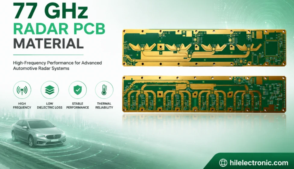
Highleap requests the RF-critical dimensions, stackup, copper, finish, mask openings, antenna keep-outs and test structures before CAM release. We distinguish critical mmWave features from ordinary mechanical dimensions so inspection effort is applied where it matters.
Hybrid construction
Premium RF material can be limited to antenna or RF layers, with lower-cost material on digital and power layers. This must be engineered as a complete stack—not assembled from independently acceptable materials.
Ground and shielding
Via fences, edge plating, cavities and reference transitions may be needed to control modes and isolation. Their dimensions and plating requirements must be explicit.
Repeatability is the main manufacturing test. A prototype can work even when the process window is broad, but volume production exposes variation in material lots, copper distribution, panel loading and plating. We place etch compensation for critical geometry, PTFE or low-loss material process control, coupon and panel-scaling strategy and RF stackup confirmation in the production release to provide a stable comparison between lots.
Many radar boards combine the antenna, RF front end, control logic and power functions in one compact assembly. The stackup must keep the antenna reference environment stable while providing practical escape and power distribution for packaged components. If a hybrid stackup is used, the bonding system, lamination temperature, material movement and copper balance must be reviewed together to avoid registration error or warpage.
Highleap 77 GHz Radar PCB Manufacturing Advantages
Highleap provides RF and microwave PCB manufacturing, hybrid lamination, fine-line imaging, controlled impedance, laser drilling, via-in-pad, back drilling, plated cavities, edge plating and low-loss finishes. Inspection can include AOI, dimensional measurement, electrical test, cross-section, impedance and optional RF coupon characterization.
Final capability depends on the exact material, thickness, panel size and antenna geometry.
The approved manufacturing data are retained for repeat orders. Material identity, scaling, drill route, plating target and inspection method remain under change control. This protects the product from antenna resonance shift or excess feed loss caused by an undocumented process or supply change.
A capability claim has value only when it is connected to a controlled shop-floor route. Highleap links RF stackup confirmation, etch compensation for critical geometry, PTFE or low-loss material process control and coupon and panel-scaling strategy to incoming inspection, lamination, drilling, plating, imaging and final verification. The exact sequence remains subject to the approved material and board construction.
77 GHz Radar PCB Assembly
Radar assembly can include fine-pitch ICs, RF packages, connectors, shields, heat spreaders and mechanical housings. Highleap supports SPI, SMT, BGA/LGA placement, controlled reflow, AOI, X-ray, selective soldering and customer-defined functional testing.
Assembly review must protect antenna surfaces, control board warpage, avoid contamination and maintain connector or housing alignment.
One project engineer coordinates fabrication and SMT questions. This avoids a common failure in which the PCB is optimized without considering assembly, or the assembly plan assumes pad, warpage and thermal conditions that the bare-board construction cannot reliably provide.
Inspection is selected by package and defect risk. SPI controls paste deposition, AOI checks visible placement and solder features, and X-ray is used where joints are hidden. Special optical, RF or mechanical interfaces may also require fixtures, datum checks or customer handling instructions.
Assembly can change the RF environment even when the bare board is within tolerance. Solder volume, package seating, shields, radomes, housings and nearby metal can affect transitions or antenna behavior. Highleap controls the PCB assembly operations that are part of the agreed process and uses customer drawings or fixtures for product-specific mechanical references. Full radar calibration remains a system-level activity unless a defined test method is included in the project.
Start the 77 GHz Radar PCB Review with the Board Files
Send the Gerber files or PCB design files first. You do not need to identify every RF tolerance, copper option or material property before contacting Highleap. When fabrication notes are already embedded in the Gerber package, they are sufficient for the first review.
Our radar PCB engineers identify the critical items
Your assigned engineer will review antenna and feed-line geometry, dielectric construction, copper, solder mask, surface finish and assembly areas with our RF manufacturing team. We will contact you directly to confirm only the decisions that affect performance or production. This keeps the quotation process simple for purchasing while preserving the technical control required at 77 GHz.
Purchasing is not expected to complete a signal-integrity, RF or lamination questionnaire before contacting us. After reviewing the board files, we ask focused questions about low-profile copper, antenna and feed-line dimensional accuracy, stable Dk and low Df or controlled dielectric thickness only when they change feasibility, price, delivery or acceptance.
77 GHz Radar PCB Cost Factors
Cost is driven by RF laminate, low-profile copper, hybrid lamination, thin dielectric control, fine etch, antenna inspection, plated features, test coupons, automotive documentation and production volume. The cheapest raw laminate can produce the highest total cost if it requires unstable processing or poor yield.
For prototype-to-volume planning, yield matters more than unit material price alone. Features that create connector or package transition mismatch or excess feed loss can increase scrap and rework. A stable, documented construction often produces a lower total cost than an aggressive design that requires repeated engineering changes after assembly.
The quotation reflects the complete route required to achieve acceptable yield. Major drivers include special laminate, copper profile, thin dielectric control, critical-feature inspection, panel yield and RF testing. Material price is only one component; extra lamination, special drilling, tight registration, inspection time and test coupons can have an equal or larger effect.
The Best Radar Material Is the One That Can Be Repeated in Production
At 77 GHz, material selection and PCB fabrication cannot be separated. Highleap helps translate the approved RF model into a controlled board and assembled radar module while the laminate supplier remains responsible for the base material.
Generic datasheet values are not enough when ordinary electrical testing cannot detect excess feed loss or phase imbalance across channels. The review must use the exact core or prepreg, copper profile, finished thickness and via route. This is where one-to-one engineering support prevents the buyer from having to interpret multiple supplier documents alone.
A laboratory result has limited value if the material thickness, copper profile or critical geometry cannot be held in later lots. The production release should identify the exact construction, RF-critical dimensions, allowed substitutions and acceptance method. Highleap keeps those details under change control so a repeat order is not treated as a fresh interpretation of the material name.
Frequently Asked Questions
Does Highleap manufacture 77 GHz radar laminate?
No. Highleap manufactures PCBs and PCBAs using verified materials from approved laminate suppliers.
Which is better for 77 GHz: PTFE or hydrocarbon ceramic?
Neither is universally better. Compare loss, Dk stability, copper, thickness, temperature, processing and cost for the actual design.
Can a 77 GHz board use a hybrid RF/FR-4 stackup?
Yes, when lamination compatibility, registration, CTE, bonding and electrical performance are qualified.
Should solder mask cover radar antenna structures?
It depends on the RF design. The mask rule must be included in the electromagnetic model and fabrication drawing.
Can Highleap assemble automotive radar boards?
Yes, subject to BOM, package, process, inspection, traceability and qualification requirements.
Do I need to choose every radar material property before requesting a quote?
No. Send the Gerber files or PCB design files first. A Highleap engineer will review the RF structure with our technical team and help confirm the material, copper and fabrication details that actually matter.
Technical reference note: Material properties and interface descriptions must be checked against the current manufacturer datasheet, customer specification and applicable interface standard for the exact production construction. Highleap Electronics is the PCB fabrication and PCB assembly provider; laminate and component trademarks belong to their respective manufacturers.

Recommended Posts

Isola Astra MT77 PCB Manufacturing
Figure 1. Isola Astra MT77 PCB ManufacturingIsola Astra...

Nelco N4000-13 PCB Material and Manufacturing Guide | Highleap Electronics
Figure 1. Nelco N4000-13 PCBNelco N4000-13 PCB is a...

Copper Clad Laminate: Complete Material Selection Guide for PCB Engineers
Every electrical property that matters in a printed...

Inside a China Ceramic PCB Factory: Process Control Across Power/LED/RF/Medical
Table of Contents Inside a China Ceramic PCB Factory: How...
How to get a quote for PCBs
Let’s run DFM/DFA analysis for you and get back to you with a report. You can upload your files securely through our website. We require the following information in order to give you a quote:
-
- Gerber, ODB++, or .pcb, spec.
- BOM list if you require assembly
- Quantity
- Turn time
For PCBA services, please provide your BOM (Bill of Materials) and any specific assembly instructions. We also offer DFM/DFA analysis to optimize your designs for manufacturability and assembly, ensuring a smooth production process.