
Taconic TLY PCB Price and PCBA Quotation
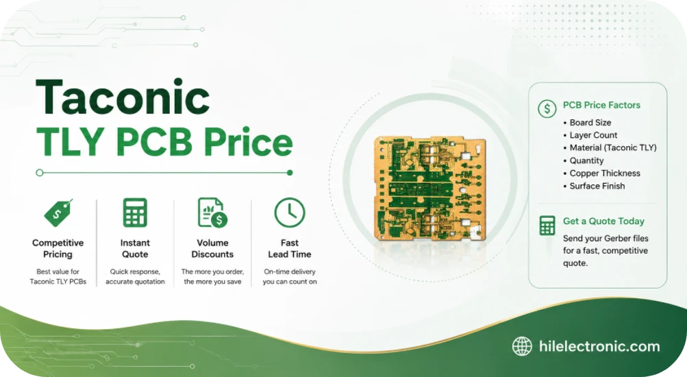
Highleap Electronics provides Taconic TLY PCB price quotations for 77 GHz radar, mmWave antennas, satellite RF, aerospace modules and low-loss microwave products. Quotes can include the exact TLY laminate, precision PCB fabrication, first-article inspection, component sourcing, RF assembly, X-ray, customer-defined testing, packing and delivery.
There is no single valid TLY unit price. TLY-3, TLY-5, TLY-5A, TLY-5Z and legacy constructions differ in dielectric data, thickness availability, copper, panel handling, PTH reliability, material yield and application. Highleap prices the released grade and process rather than grouping the family under one generic rate.
TLY-3, TLY-5 and TLY-5Z Price-Relevant Differences
Current AGC data positions TLY-3 and TLY-5 as very-low-Dk, low-loss woven-glass PTFE materials for radar, satellite, cellular and aerospace applications. TLY-5Z uses a glass-filled woven structure designed for lower Z-axis expansion and improved plated-through-hole stability. Selecting among them changes both electrical design and manufacturing cost.
| Current grade | Published data / positioning | Primary quotation impact |
|---|---|---|
| TLY-3 | Dk 2.33 ± 0.02; Df 0.0012; very-low-Dk RF/mmWave material. | Exact thickness, copper, panel yield, fine geometry and RF acceptance scope. |
| TLY-5 | Dk 2.2 ± 0.02; Df 0.0009; ultra-low-loss material used for 77 GHz and mmWave. | Thin-material handling, copper profile, critical dimensions and test requirements. |
| TLY-5Z | Dk 2.2 ± 0.04; Df 0.0015; low-Z-axis material with PTH-stability positioning. | PTH construction, thickness, mechanical requirements and approved electrical model. |
| Legacy/other TLY | Use the controlled customer datasheet and approved source. | Supply, MOQ, certificates, qualification and possible transition cost. |
Official references: AGC TLY-3, AGC TLY-5 and AGC TLY-5Z.
Taconic TLY PCB Price by Grade and Construction
The TLY family includes different low-Dk PTFE constructions. Current AGC pages identify TLY-3, TLY-5 and TLY-5Z, with different Dk, Df, density, Z-axis behaviour and application positioning. A “TLY PCB price” therefore requires the exact grade and construction.
What the Highleap TLY Quotation Can Include
| Project area | Highleap project support |
|---|---|
| Material procurement | Exact grade, thickness, copper, MOQ, certificate and availability |
| Precision fabrication | Thin-panel handling, RF etching, PTH, mechanical features, electrical test and inspection |
| Quality evidence | Critical dimensions, first-article report, impedance/RF records and X-ray when specified |
| Assembly | Components, stencil/NRE, MMIC/QFN/BGA, RF connectors, shields and controlled cleaning |
| Testing | Programming, functional test and customer-defined radar/mmWave verification |
| Delivery/support | Prototype and volume milestones, packing, logistics, traceability and repeat-order control |
Highleap Rigid RF PCB Manufacturing Capabilities
The published factory limits below provide the baseline for a TLY price review. Thin PTFE handling, RF critical dimensions, low-profile copper, panel support and testing can narrow the practical process window for a specific TLY construction. See the complete Highleap rigid PCB capability table for the published factory specification.
| Manufacturing item | Published Highleap capability | RF/PTFE project condition |
|---|---|---|
| Maximum layer count | Up to 60 layers | Layer count for a specific RF/PTFE or hybrid stackup is confirmed after lamination, registration, via and material review. |
| Minimum inner-layer trace/space | 2/2 mil (0.05/0.05 mm) | The released RF geometry also depends on copper thickness, foil type, etch compensation and critical-dimension tolerance. |
| Minimum outer-layer trace/space | 2/2 mil (0.05/0.05 mm) | Fine RF gaps and coupled structures require project-specific feasibility and inspection criteria. |
| Board thickness range | 0.2–8.0 mm | Available thickness for a named Taconic/AGC construction depends on laminate gauge, bonding method and approved stackup. |
| Board-thickness tolerance | ±0.1 mm below 1.0 mm; ±10% at 1.0 mm and above | RF connector launches and enclosure interfaces should state any tighter product-level requirement. |
| Minimum finished board size | 10 × 10 mm | Small circuits may require delivery in a manufacturing panel or array for fabrication and assembly. |
| Maximum finished board size | 22.5 × 47.5 in (571.5 × 1206.5 mm) | Large-format PTFE boards require separate review for material sheet size, registration, flatness, routing and shipment. |
| Minimum mechanical drill / annular ring | 0.15 mm / 0.127 mm | Final via design depends on board thickness, aspect ratio, plating requirement and material-specific drilling process. |
| Minimum laser drill / annular ring | 0.075 mm / 0.075 mm | Laser microvias are subject to dielectric thickness, capture-pad design, copper build and sequential-lamination review. |
| Mechanical-drill aspect ratio | Up to 20:1 | The achievable ratio for an RF/PTFE build must be confirmed with finished hole size, board thickness and plating requirement. |
| Laser-drill aspect ratio | 1:1 | Microvia geometry is released only after stackup and reliability review. |
| Maximum inner/outer copper | Up to 10 oz | Maximum copper cannot automatically be combined with the finest trace/space or every PTFE construction. |
| PTH / NPTH tolerance | PTH ±0.075 mm; NPTH ±0.05 mm | Connector and RF grounding holes should identify finished diameter and any tighter fit requirement. |
| Contour tolerance | ±0.1 mm | Edge launches, cavities, slots and connector locations may need a dedicated dimensional-control plan. |
| Controlled-impedance tolerance | Single-ended and differential: ±5 Ω at ≤50 Ω; ±7% above 50 Ω | The quoted tolerance applies to an approved stackup, coupon strategy and measurement method. |
| Available surface finishes | ENIG, ENEPIG, OSP, HASL, immersion silver, immersion tin, flash gold, hard gold and gold fingers | Finish selection is reviewed for RF loss, soldering, wire bonding, connector contact and environmental requirements. |
Capability-combination notice: values in the table are individual factory capability limits. Layer count, 2/2 mil geometry, 10 oz copper, maximum panel size, 20:1 aspect ratio and the thinnest board construction are not assumed to be simultaneously achievable. Highleap confirms the usable combination after reviewing the exact material, stackup, copper, drill, RF tolerance, surface finish and assembly package.
| Example family member | Published positioning | Commercial implication |
|---|---|---|
| TLY-3 | Very-low-Dk woven-glass PTFE material, Dk 2.33 ±0.02 | Different geometry and stock from Dk-2.2 grades. |
| TLY-5 | Very-low-Dk, very-low-loss material, Dk 2.2 ±0.02 | Common in mmWave/radar discussions; thickness and copper still control price. |
| TLY-5Z | Low-Dk, lower-Z-axis-expansion and low-density construction | May be selected for PTH stability or lightweight applications; not priced as standard TLY-5. |
| Legacy or customer code | May refer to older TLY designation or internal specification | Requires controlled TDS and approved source before quotation. |
Highleap states grade, thickness, copper, source, certificate requirements and allowed alternatives in the quotation. No TLY family member is substituted only because its name or nominal Dk is close.
Material Thickness, Copper, and Panel Utilisation
TLY price is strongly affected by laminate thickness and copper option. Thin mmWave cores, low-profile/rolled copper and nonstandard sheet configurations may have different availability, minimum purchase and handling yield.
Separating Material Price from Manufacturing Risk
A lower laminate price does not guarantee a lower finished PCB cost if the construction reduces panel yield, requires tighter handling, adds PTH risk or changes RF test requirements. Highleap itemises those drivers and can compare TLY options with specialty low-loss laminate PCB cost or other approved material routes when the design owner permits alternatives.
- exact dielectric thickness and tolerance;
- copper foil type, weight and surface profile;
- finished board dimensions and quantity per production panel;
- tooling rails, coupons, fiducials and assembly panel requirements;
- board orientation where woven structure or antenna geometry matters;
- usable yield after routing, test coupons and edge-launch features.
Highleap reviews material use together with the high-frequency PCB cost model and RF copper foil selection. Cost-down suggestions focus on standard available constructions and better panel use, not an unapproved change in electrical performance.
Fabrication and Quality Costs for TLY Circuits
TLY fabrication cost reflects more than the PTFE sheet. Thin-material handling, precision imaging, etch compensation, plated-through-hole preparation, laser features, hybrid lamination, routing support and RF evidence can be significant.
| Cost area | Why it is required | How to control it |
|---|---|---|
| Precision RF imaging/etch | mmWave geometry can be sensitive to small dimensional changes | Identify only the truly critical features and measurable tolerances. |
| PTH or via processing | Material-specific preparation and hole reliability | Use manufacturable hole/aspect ratios and defined microsection scope. |
| Hybrid lamination | Bonding system, flow, pressure and registration | Provide a released stackup and avoid unnecessary press cycles. |
| RF coupons/test | Validates impedance, loss or phase requirements | Agree test method and sampling before tooling. |
| Mechanical support | Thin panels need fixtures and protective handling | Design robust panel rails and shipping support. |
| Quality documentation | Traceability, FAI, dimensional and electrical records | Specify contractually required evidence rather than generic reports. |
Highleap’s RF tolerance process and RF PCB testing options are used to define the required production evidence.
TLY Prototype, NPI, and Volume Cost Planning
Prototype TLY pricing includes material minimum, engineering, tooling and setup across a small quantity. NPI adds first-article review, assembly learning and test development. Volume cost can improve with forecast purchasing, repeat tooling, panel optimisation and stable release schedules.
| Stage | Primary cost focus | Highleap quotation output |
|---|---|---|
| Prototype | Minimum material and fast engineering feedback | Standard and expedite options with basic evidence. |
| RF validation | Critical dimensions, coupons, connector launches and RF test | First-article plan and separate test/NRE. |
| PCBA pilot | BOM availability, stencil, fixture, inspection and programming | Bare board, setup, assembly and test breakdown. |
| Volume | Panel yield, material forecast, component pricing and delivery cadence | Quantity breaks and scheduled-release pricing. |
| Long-life programme | Material continuity, change control and traceability | Reservation/second-source strategy subject to approval. |
PCBA cost is developed from the BOM and package mix using PCB assembly cost factors and Highleap’s turnkey PCB assembly service.
Lead Time: Material and Test Often Set the Critical Path
TLY lead time depends on exact grade, thickness, copper, required quantity, fabrication complexity, assembly components and RF test. Highleap confirms those items before committing a date.
Highleap confirms quotation timing after material availability, fine-feature feasibility, assembly component status and test preparation are known. Expedited fabrication, first-article assembly and production shipment are priced and scheduled as separate deliverables where that lowers programme risk.
- priority material and fabrication review through quick-turn PCB manufacturing;
- bare-board-first or first-article shipment for early RF validation;
- separate assembly milestone when components or fixtures have longer lead time;
- split quantity delivery when production validation can begin before the full order;
- forecast and reserved-material planning for repeat demand.
A quotation identifies the date assumptions and any customer action needed to hold the schedule, such as stackup approval, component-alternate approval, test-fixture release or acceptance of a split shipment.
Request a TLY PCB Price and PCBA Schedule
Send exact TLY grade, material/thickness/copper requirement, Gerber/ODB++, fabrication drawing, stackup, RF geometry or impedance, drill/route data, surface finish, quantities, target date, delivery location, BOM, centroid, assembly drawings, firmware and test specification through Highleap quick quote or contact Highleap.
For TLY-5 mmWave manufacturing, review TLY-5 PCB manufacturing. For comparing other RF laminates, use RF PCB material comparison.
Can Highleap quote TLY PCB price from only board dimensions?
A rough budget may be possible. A firm price requires exact grade, dielectric thickness, copper, fabrication data, quantity, finish and quality/test scope.
Which TLY grade is cheapest?
There is no universal answer. Grade, thickness, copper, stock, panel yield, process and qualification determine total cost.
Can Highleap provide a fast TLY prototype?
Expedited production may be available after material and engineering release. The quote states committed milestones for fabrication and assembly.
Can Highleap include RF assembly and testing?
Yes. The BOM, package risks, fixture, calibration, frequency and acceptance limits must be provided or quoted as test development.
What data is required for a firm TLY PCB price?
Provide exact grade, thickness, copper, Gerber/ODB++, drawing, stackup, critical RF dimensions, quantities, target delivery, BOM, assembly drawings and test requirements.
Can Highleap propose cost reduction without changing RF performance?
Highleap can review panel utilisation, standard material constructions, tolerance allocation, inspection level, split delivery and assembly packaging. Any material, thickness, copper or electrical change requires customer approval before quotation release.

Recommended Posts

Isola Astra MT77 PCB Manufacturing
Figure 1. Isola Astra MT77 PCB ManufacturingIsola Astra...

Nelco N4000-13 PCB Material and Manufacturing Guide | Highleap Electronics
Figure 1. Nelco N4000-13 PCBNelco N4000-13 PCB is a...

Copper Clad Laminate: Complete Material Selection Guide for PCB Engineers
Every electrical property that matters in a printed...

Inside a China Ceramic PCB Factory: Process Control Across Power/LED/RF/Medical
Table of Contents Inside a China Ceramic PCB Factory: How...
How to get a quote for PCBs
Let’s run DFM/DFA analysis for you and get back to you with a report. You can upload your files securely through our website. We require the following information in order to give you a quote:
-
- Gerber, ODB++, or .pcb, spec.
- BOM list if you require assembly
- Quantity
- Turn time
For PCBA services, please provide your BOM (Bill of Materials) and any specific assembly instructions. We also offer DFM/DFA analysis to optimize your designs for manufacturability and assembly, ensuring a smooth production process.