
7 Key Design Challenges in Drone Optical Data Link PCBs

The drone optical data link PCB is the electro-optical conversion engine at the center of every fiber-tethered UAV communication chain. It translates electrical signals from the flight computer into modulated laser light for fiber transmission, and performs the reverse conversion on incoming optical signals — turning received photons back into electrical data the processor can act on. Every other board in the tether system — the spool controller, the canister electronics, the ground station — depends on this one component performing its conversion with enough fidelity that the entire link meets its data rate, latency, and bit-error-rate targets.
What makes optical data link PCB design demanding is the coexistence of incompatible signal environments on a single board: gigabit-rate differential signals from the FPGA, a precision analog laser drive circuit sensitive to microvolt-level noise, a low-noise photodetector front end operating at the edge of its sensitivity, and multiple power domains that must be isolated from each other while sharing a compact substrate.
Get an Optical Data Link PCB Quote
Quick answer
A drone optical data link PCB converts electrical data to modulated light for fiber transmission and reverses the process for incoming signals. It hosts the transceiver module, manages high-speed SerDes routing, provides precision low-noise power to the laser transmitter, and monitors link health in real time. The design determines achievable data rate, latency, and BER for the entire fiber optic drone communication path — making it the most signal-integrity-critical board in the tether stack.
Table of Contents
- System Role and Signal Flow
- Transceiver Selection: SFP, Soldered TOSA/ROSA, and Custom
- High-Speed Signal Integrity at 10 Gbps
- Laser Power Supply Design
- Receive Path and Photodetector Front End
- DDM Diagnostic Monitoring
- Layer Stack and Impedance Planning
- Thermal Management
- Manufacturing, Assembly, and Test
- Platform-Specific Design Variants
- FAQ
System Role and Signal Flow
The optical data link PCB sits at the interface between the UAV’s digital subsystem and the fiber. Its position in the tether chain determines the signal integrity budget for everything upstream and downstream: whatever optical power margin the transceiver achieves, whatever timing jitter the SerDes introduces, whatever BER the clock recovery circuit produces — these parameters bound what the ground station can recover.
Signal flow on the transmit path: the FPGA generates differential LVDS or CML data at line rate → the SerDes serializer converts parallel data to a high-speed serial stream → the transceiver’s laser driver modulates the laser diode → the fiber carries optical power to the ground station. The receive path mirrors this: incoming optical power → photodetector → transimpedance amplifier → limiting amplifier → CDR (clock and data recovery) → FPGA deserializer → parallel data to the processor.
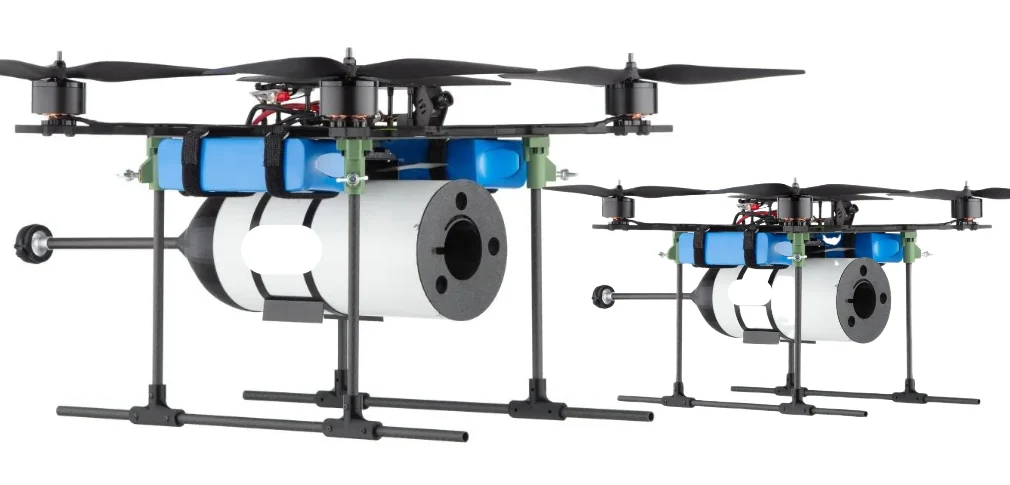
The board must manage all of this in a UAV environment: vibration across the 10–2000 Hz range, temperature swings from −20 °C at altitude to +60 °C in direct sun, connector shock from landing, and the chronic constraint of weight budgets measured in grams. These requirements shape every decision from transceiver selection to PCB material choice. The UAV tether PCB system places additional mechanical constraints on connector orientation and board form factor.
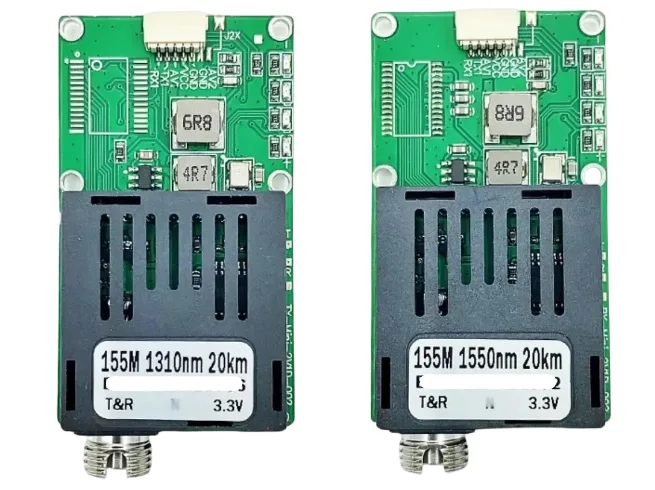
Transceiver Selection: SFP, Soldered TOSA/ROSA, and Custom
The transceiver selection decision has more downstream consequences than any other choice in optical data link board design. It determines connector type, cage geometry, footprint, thermal path, supply interface, and — critically — whether field replacement is possible.
| Type | Data Rate | Weight Penalty | Field Serviceability | Best Application |
|---|---|---|---|---|
| Pluggable SFP | up to 1 Gbps | ~8–12 g (cage + module) | Yes — swap in field | Commercial tethered drones, development platforms |
| Pluggable SFP+ | up to 10 Gbps | ~10–15 g | Yes | Multi-camera 4K surveillance, high-bandwidth ISR |
| Soldered TOSA/ROSA | application-defined | ~2–4 g | No — board-level replacement | Weight-critical platforms, OEM integrated products |
| Custom VCSEL array | 25 Gbps+ per lane | Substrate-integrated | No | Defense programs needing supply chain independence and maximum bandwidth |
For pluggable SFP/SFP+ designs, cage selection matters beyond the electrical interface. EMI gaskets, retention force, and vibration rating vary between cage manufacturers. Aviation-rated cages with locking mechanisms are appropriate for any UAV that undergoes significant maneuvering. The cage should be thermally coupled to the PCB through thermal vias to a copper pour, not left to convect in air.
Soldered TOSA/ROSA designs eliminate the mechanical complexity of the cage but require the designer to define the electrical interface to the laser driver and TIA directly. The advantage is a 3–6 g weight reduction and elimination of the cage’s vibration sensitivity — relevant for platforms where connector integrity under vibration is a concern.
High-Speed Signal Integrity at 10 Gbps
At 10 Gbps, the unit interval is 100 ps. A via transition that adds 15 ps of delay asymmetry between a differential pair degrades the eye opening measurably. Routing decisions that would be acceptable at 1 Gbps produce marginal links at 10 Gbps and open failures at 25 Gbps. The optical data link board is where signal integrity discipline must be most rigorous across the entire drone PCB stack.
Differential impedance control: 100 Ω ±10% for SFP/SFP+ host interface (IEEE 802.3 requirement). Achieved through controlled trace geometry — typically 100 µm traces with 100 µm spacing on FR-4, tighter on low-loss materials. Every layer transition requires a reference return via within 200 µm of each signal via.
Via stub management: On boards thicker than 1.6 mm, a via through the full stackup creates a stub below the signal layer that resonates in the 10–20 GHz range, producing insertion loss notches and reflections. Back-drilling removes the stub to within 125 µm of the signal layer. For high-volume production, blind or buried vias eliminate the stub by design — the via only exists between the layers it needs to connect. The choice between back-drilling and blind/buried vias depends on board thickness, volume, and cost tolerance.
Layer assignment: Route high-speed differential pairs on stripline layers (inner layers between reference planes) rather than microstrip. Stripline has symmetric return current distribution and is shielded from radiated emissions. Never route a 10G pair adjacent to a power plane — the impedance discontinuity where the plane splits or changes voltage produces reflections that open the eye.
AC coupling: The SFP+ specification requires AC coupling on the host side, 100 nF in 0402 package, placed within 5 mm of the SFP+ pads. Low-ESL capacitors are required — standard multilayer ceramics in X5R/X7R dielectric. The coupling capacitors also serve as the DC block preventing laser bias current from flowing into the FPGA SerDes.
For FPGA-based designs, the differential pairs leaving the FPGA BGA fanout zone require particular attention. BGA via fields create a capacitive loading discontinuity. The designer must choose between routing through the via field (acceptable if the field is sparse) or routing around it (necessary for dense arrays). Either way, matched length within 50 µm between the P and N traces of each pair is required from BGA pad to SFP cage pad. The HDI PCB approach using microvias reduces via stub concerns while enabling tighter BGA fanout.
Laser Power Supply Design
Why laser power supply noise matters more than any other supply on the board
The laser diode is a linear converter from electrical current to optical power. Supply ripple at any frequency within the modulation bandwidth appears directly as amplitude modulation on the optical output. At 10 Gbps, the modulation bandwidth extends to 7 GHz — meaning ripple anywhere from DC to 7 GHz degrades the optical SNR. Switching converter noise at 1–5 MHz, ground bounce from FPGA switching at 100–500 MHz, and even thermal EMF from temperature gradients all contribute to this noise floor. The power supply design is not a secondary concern — it is a primary determinant of optical link quality.
The preferred architecture: a switching converter provides an intermediate bus (3.3 V or 5 V), followed by dedicated low-noise LDOs for each transceiver voltage rail. A ferrite bead with high impedance at 100 MHz–1 GHz isolates the LDO input from the switching converter output. The LDO output connects to the transceiver through a filter: 22 µF bulk ceramic + 100 nF bypass + 100 pF high-frequency decoupling, all within 3 mm of the module power pins.
Transceiver voltage domains: standard SFP modules require 3.3 V at up to 1 A. SFP+ modules may require separate 3.3 V supply and a 1.8 V supply for internal logic. The two supplies must be sequenced — logic before power amplifier — per the module’s datasheet power-up sequence. Incorrect sequencing damages laser drivers. Sequencing is implemented in hardware (RC delay circuits or a dedicated sequencer IC) rather than relying on software startup order, which is unreliable in fault recovery scenarios.
Ground return current deserves the same attention as the supply. The laser drive current return path must be a direct, low-impedance connection to the ground reference of the transmitter IC. Any inductance in the return path adds to the effective laser drive impedance and reduces modulation bandwidth. Use a solid copper polygon directly beneath the laser driver, tied to the ground plane through multiple vias, rather than a routed ground trace.
Receive Path and Photodetector Front End
The receive path begins at the SFP cage’s RD± pins (or the ROSA’s electrical output) and ends at the FPGA SerDes RX differential input. The signal chain is: photodetector → TIA (transimpedance amplifier, inside the module) → limiting amplifier → CDR → FPGA input. In pluggable SFP architectures, the TIA and limiting amplifier are inside the module and the designer only needs to provide a clean AC-coupled differential path to the FPGA. In ROSA-based designs, the TIA may be an external component on the PCB.
Receiver sensitivity for a typical SFP module is −22 dBm minimum. At 10G (SFP+), −9.9 dBm is typical for SR optics. The optical power budget — transmit power minus all optical losses (fiber, connectors, splices) minus the minimum receive sensitivity — is the link margin. For a 1 km tether application with 0.4 dB/km fiber loss and two connectors at 0.3 dB each, total optical loss is under 2 dB — well within the 12+ dB budget of typical SFP+ optics.
The receive path PCB layout must minimize differential skew and capacitive loading on the RD± traces. Any asymmetry between the P and N traces translates to timing skew at the FPGA input, degrading eye opening. Avoid placing vias or topology changes on one trace of the pair without a matched change on the other. The CDR in the FPGA SerDes can tolerate some jitter, but not unlimited — the physical layer must deliver clean signals to keep the CDR locked across the operating temperature range.
DDM Diagnostic Monitoring
SFP/SFP+ modules implement Digital Diagnostics Monitoring (DDM, also called Digital Optical Monitoring or DOM) per SFF-8472. The I2C interface at address 0x51 provides real-time readback of: laser transmit power (dBm), received optical power (dBm), laser bias current (mA), module temperature (°C), and supply voltage (V). Each parameter has software-configurable alarm and warning thresholds.
DDM data is not only useful for field diagnostics — it enables predictive maintenance. Rising laser bias current while transmit power holds steady indicates laser aging (the driver is compensating for reduced efficiency). Declining received optical power with stable transmit power indicates fiber or connector degradation. Tracking these trends over flight hours allows operators to schedule maintenance before a marginal link becomes a failed link.
The I2C bus for DDM must be routed carefully. The SFP+ cage’s I2C pins are at 3.3 V logic. If the FPGA or microcontroller I2C is at a different voltage, level translation is required. The bus should have pull-up resistors to 3.3 V (typically 4.7 kΩ) and should not share the I2C bus with other devices that could introduce glitches causing the module to misconfigure. The ground-side monitoring counterpart runs on the fiber optic canister PCB, enabling end-to-end link health visibility from both ends simultaneously.
Layer Stack and Impedance Planning
A 6-layer stack is the minimum for a 10 Gbps optical data link board with adequate signal integrity and power distribution. An 8-layer stack is preferred for designs with dense BGA routing, multiple power domains, or co-located analog and digital circuitry.
Typical 6-layer assignment: Layer 1 — top components and microstrip signals; Layer 2 — ground reference plane; Layer 3 — high-speed stripline pairs (FPGA to SFP cage); Layer 4 — power planes; Layer 5 — ground; Layer 6 — bottom components and secondary signals. The two ground planes (L2 and L5) provide return paths for high-speed signals on L3 and shield the power distribution on L4 from radiating upward into the signal layers.
For designs requiring controlled impedance, the fabricator must know the dielectric constant and thickness of each prepreg/core pair, the target impedance for each layer, and the tolerance (±10% for most optical link applications, ±5% for the most demanding). TDR testing of production boards verifies actual impedance against design targets. Specifying controlled impedance in the fabrication notes — not just drawing the traces at the calculated width — is required for consistent manufacturing.
Material selection beyond standard FR-4 becomes relevant at 10 Gbps and above. FR-4 (Dk ~4.2–4.5 at 1 GHz, rising at low frequency) introduces frequency-dependent delay that degrades edge rates on long runs. For board runs longer than 100 mm at 10 Gbps, low-loss materials such as Isola 370HR or Panasonic Megtron 6 reduce insertion loss. At 25 Gbps, low-loss materials are required, not optional.
Thermal Management
SFP modules dissipate 0.5–1.5 W depending on type and data rate. SFP+ modules dissipate up to 2.5 W. In an enclosed UAV housing with limited airflow, this heat must be conducted into the PCB and then to the airframe rather than relying on convection.
The SFP cage provides a thermal interface through its top surface if designed for it — a compliant thermal interface material (TIM) between the cage lid and the UAV housing conducts module heat directly to the chassis. The cage-to-PCB interface uses thermal vias: 0.3 mm drill diameter, 1 mm pitch, arranged in a grid beneath the cage footprint. Inner layer copper pours collect heat from the vias and spread it laterally before it reaches the edge of the board or the chassis mount points.
For soldered TOSA/ROSA devices, the smaller footprint concentrates the heat dissipation over a smaller area, increasing local thermal resistance. The via array beneath soldered optics requires tighter pitch (0.6 mm) and larger copper pads to compensate. Junction temperature must be verified against the device’s maximum specification across the full operating temperature range — the combination of ambient temperature at sea level and self-heating may approach limits faster than the designer expects.
Thermal simulation is justified for this board: a 2D thermal model showing temperature distribution across the board under maximum dissipation at maximum ambient temperature takes a few hours and can prevent a return to layout late in the program. The PCB design phase is the right time to discover thermal issues, not during environmental qualification testing.
Manufacturing, Assembly, and Test
Controlled impedance with TDR verification is the mandatory fabrication requirement for optical data link boards at 10 Gbps. The fabricator measures actual trace impedance on coupons from each panel and provides documentation — not just a statement that controlled impedance was attempted. Tolerance stack-up in FR-4: ±10% is achievable; ±5% requires a premium material and tighter process control.
BGA assembly for FPGA devices requires:
- Solder paste printing with a stencil aperture ratio appropriate for the pitch — typically 0.8 mm pitch BGA uses 0.45 mm aperture diameter on a 0.15 mm stencil
- Reflow profile matching the BGA supplier’s specification — typically a ramp-to-soak at 150–170 °C followed by a soak and then ramp to peak at 240–250 °C
- X-ray inspection of all BGA joints to verify reflow and detect bridging or voids
- Acoustic microscopy for Class 3 applications to detect subsurface voiding
SFP cage assembly requires checking cage coplanarity before reflow — a cage that rocks on the PCB will not solder all ground pins reliably and will introduce resonances in the EMI gasket. The cage retention clips must engage the module with the specified insertion and extraction force; worn cages from handling during bring-up should be replaced before final assembly.
Functional test for the optical data link board: connect a fiber loopback (TX output → attenuator set to simulate link budget → RX input), apply a PRBS pattern at line rate, and measure BER over a statistically valid interval. A BER below 1×10⁻¹² with 3 dB additional attenuation beyond the link budget confirms adequate margin. Highleap provides controlled impedance fabrication and precision assembly for optical data link boards with full documentation traceability.
Platform-Specific Design Variants
Commercial surveillance tether: SFP+ at 10 Gbps, pluggable for field serviceability, standard FR-4 with back-drilling, 6-layer stack, DDM monitoring via microcontroller. The fiber optic drone circuit board in this category is well-served by commercial-off-the-shelf SFP+ optics with standard cage assemblies.
Fiber-guided expendable platform: TOSA/ROSA soldered, single-use reliability qualification (functional test plus burn-in, no conformal coating required), cost-optimized layer count. The fiber-guided UAV control PCB requires the optical data link board to operate reliably from ambient start to end of mission — usually 30–90 minutes — without the ongoing diagnostic monitoring needed for reusable platforms.
Defense ISR platform: Polyimide substrate, IPC Class 3 assembly, conformal coating, MIL-STD-810 environmental qualification, potentially custom transceiver for supply chain independence. Detailed requirements for this category are in the military fiber drone PCB context.
FPV racing/close-range: 1 Gbps SFP sufficient, lightweight design priority, shorter tether means lower optical loss budget allows use of multimode fiber and 850 nm VCSEL transceivers (lower cost, higher power output, less wavelength-sensitive). The fiber optic FPV drone PCB represents this category’s design philosophy.
In all variants, the optical data link board interacts with the fiber optic tether spool PCB through the tether cable — the spool board’s tension and dispensing management directly affects fiber integrity and thus the optical power budget the data link board must accommodate.
FAQ
What data rates are typical for current UAV fiber tether systems?
Deployed commercial systems typically use 1 Gbps (SFP) or 10 Gbps (SFP+). Multi-camera 4K surveillance drones carrying multiple uncompressed streams require 10 Gbps minimum. Advanced programs are moving to 25 Gbps per lane using QSFP28 or custom VCSEL-array interfaces. Older tethered systems used 100–400 Mbps; most new designs skip these rates in favor of 1G or 10G standards with available component ecosystems.
Can the board handle multiple simultaneous video streams?
Yes — the FPGA multiplexes streams into the optical channel. Three 1080p60 uncompressed streams require approximately 9 Gbps, fitting within a 10 Gbps link with margin. Three 4K30 streams require compression or a move to 25 Gbps. The FPGA’s role in stream aggregation is separate from the optical data link board’s physical layer function, but the FPGA and optical transceiver share the same board and their layout interacts.
What determines the maximum tether length for a given board design?
Optical link budget: transmit power (typical SFP+ −1 to +3 dBm) minus connector losses (0.3–0.5 dB each) minus fiber attenuation (0.35 dB/km at 1310 nm) minus receive sensitivity (−9.9 dBm typical for SFP+ SR, −20 dBm for LR). A 1310 nm LR SFP+ with −3 dBm transmit and −20 dBm receive sensitivity yields a 17 dB budget — supporting over 40 km of fiber loss, far beyond any practical tether application. Most tether length limits are mechanical (fiber weight and spool capacity), not optical.
How does vibration affect the optical interface?
Pluggable SFP cages are sensitive to vibration through two mechanisms: the module can work loose in the cage if the retention latch is not properly engaged, and the cage-to-PCB solder joints can fatigue under prolonged vibration. Aviation-rated cages address both: they have stronger retention mechanisms and heavier ground pin arrays. For designs that will undergo significant vibration testing, it is worth specifying aviation-rated cages in the BOM rather than standard commercial cage assemblies.

Recommended Posts
Rogers TMM6 PCB Manufacturing for Microwave Filters
Table of contentsWhy Microwave Filter Designers Use...
Taconic fastRise 27 Prepreg PCB Bonding and HDI Fabrication Service
Table of contentsWhat fastRise 27 Is—and What You Are...
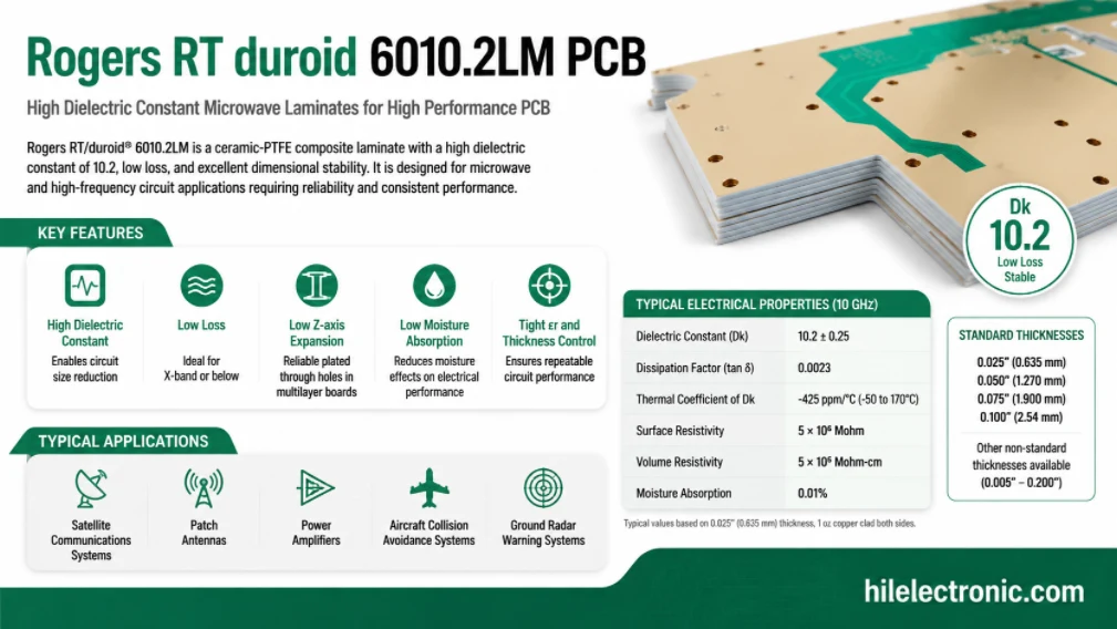
Rogers RT/duroid 6010.2LM PCB Manufacturer and Fabrication Service
Table of contentsIs RT/duroid 6010.2LM the Right Material...
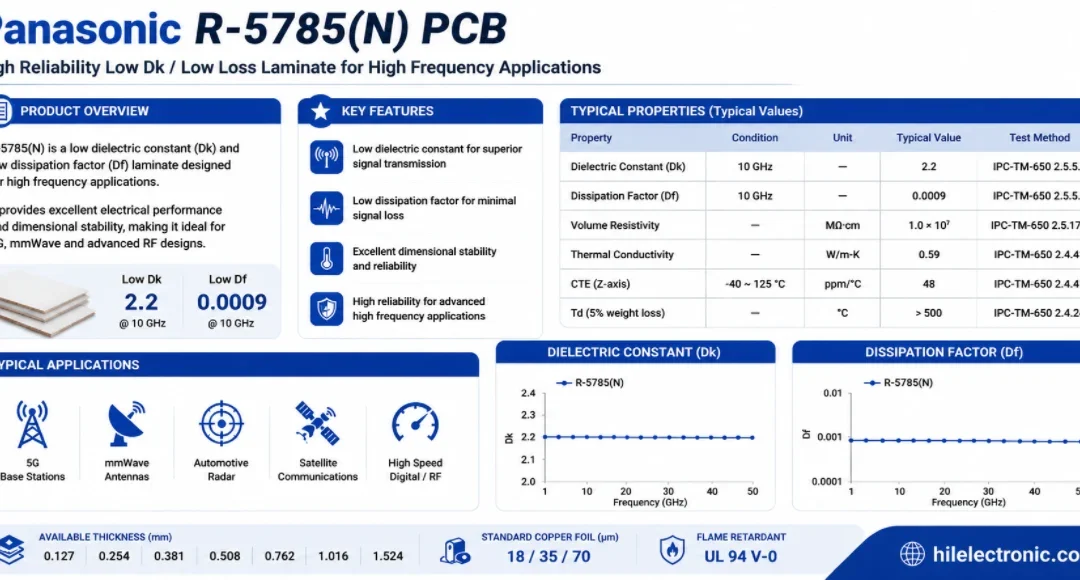
Panasonic R-5785(N) MEGTRON 7 PCB Manufacturer and Fabrication
Table of contentsWhen a Design Should Move to R-5785(N) /...
How to get a quote for PCBs
Let us run DFM/DFA analysis for you and get back to you with a report.
You can upload your files securely through our website.
We require the following information in order to give you a quote:
-
- Gerber, ODB++, or .pcb, spec.
- BOM list if you require assembly
- Quantity
- Turn time