
ITEQ IT-988GSE PCB for 56G/112G Channel Loss Control
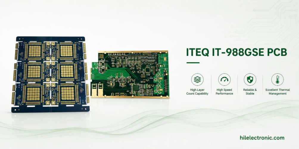
ITEQ IT-988GSE should be chosen from a quantified channel budget, not from the aggregate label on a switch, router, storage system, or backplane. “400G” does not reveal the lane rate, modulation, symbol rate, routing length, connector count, package loss, via topology, copper profile, equalization, or allowable insertion loss. Two products with the same front-panel bandwidth can place very different demands on the PCB.
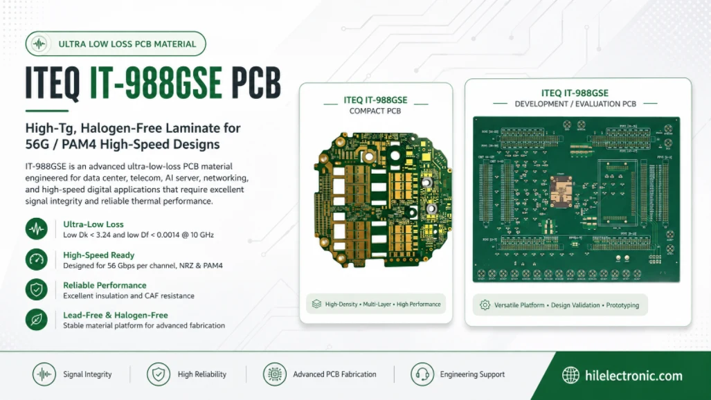
ITEQ classifies IT-988GSE as an ultra-low-loss, high-Tg, halogen-free laminate and prepreg system and currently lists typical Dk 3.21 and Df 0.0014 for the stated 10 GHz, 70% resin-content comparison. The original product launch also identified low-Dk glass, availability with ultra-low-profile copper, data rates beyond 56 Gbps per channel, Tg above 230°C, and low total expansion. These properties are valuable only after the larger discontinuities and conductor-loss sources are understood.
Why Not Every 100G, 400G, or 800G Board Needs IT-988GSE
Aggregate Ethernet generation is a system descriptor, not a laminate specification. A short line card with one connector can have abundant margin on a less expensive material, while a long orthogonal backplane path with multiple connectors and several via transitions can be loss-limited at a similar lane rate. The decision must be made per electrical path and per worst-case routing class.
The comparison becomes especially important with PAM4. A 112 Gb/s PAM4 lane typically operates near 56 GBd, so its Nyquist frequency is around 28 GHz—similar to a 56 Gb/s NRZ lane—but PAM4 uses four amplitude levels and has less vertical eye margin. That makes noise, crosstalk, reflection, and loss management more demanding even when the Nyquist frequency is not doubled. At 224 Gb/s PAM4, the symbol rate and relevant frequency range rise again, increasing the value of accurate high-frequency construction data and low-profile copper.
| Board/channel example | Do not decide from | Decide from |
|---|---|---|
| Short chip-to-chip route on one PCB | The server or switch is marketed as 400G/800G. | Actual lane rate, package model, route length, layer, copper, via transitions, receiver margin, and required manufacturing guard band. |
| Long backplane through two large connectors | Nominal Df alone. | Connector and launch S-parameters, via-stub plan, board segment lengths, copper profile, return loss, insertion-loss mask, and equalization. |
| Dense line card with BGA breakout and one midplane connector | Number of PCB layers. | Breakout discontinuity, reference-plane transitions, connector loss, crosstalk, layer-assignment loss, and process tolerance. |
| Short route with many poorly designed vias | Material tier. | Topology correction first: remove stubs, improve antipads and return vias, preserve reference continuity, then reassess residual loss. |
| Long route already optimized with VLP copper and backdrill | Brand preference. | Worst-case channel simulation and measured test vehicle showing that dielectric loss remains a material portion of the margin. |
A practical project classifies routes into families—short on-board, medium card, long card-to-card, longest backplane—and uses the worst manufacturable stackup for each family. IT-988GSE may be justified only on the longest class or only on selected layers. A blanket material callout can add cost without improving the bottleneck path.
Decompose the Channel Loss Budget Before Selecting Material
The loss budget should be a ledger, not a single insertion-loss curve with no ownership. Break the channel into packages, PCB segments, vias, connectors, AC-coupling structures, and other transitions. Assign models, temperature, and manufacturing variation to each block. The purpose is to identify which part of the channel consumes margin and which design change can recover it.
| Budget element | What to model or measure | Typical design lever |
|---|---|---|
| Transmitter and receiver packages | Package insertion/return loss, breakout, reference structure, ball-field escape. | Package-aware fanout, layer choice, pad/antipad and return-via tuning. |
| Straight PCB routing | Dielectric loss, conductor loss, copper roughness, width/thickness, glass-weave skew. | Material tier, VLP foil, wider traces where allowed, shorter routing, lower-loss layers. |
| Signal vias | Barrel inductance, pad/antipad capacitance, residual stub resonance, mode conversion. | Backdrill, blind/buried vias, optimized antipads, return vias, fewer transitions. |
| Connectors and launches | Connector loss, crosstalk, launch field conversion, reference transition. | Validated footprint, launch optimization, connector selection, fewer connector interfaces. |
| Plane changes and DC blocks | Return-path discontinuity, spreading inductance, capacitor pad discontinuity. | Continuous references, close return vias, optimized capacitor land pattern. |
| Process and environment | Etch width, dielectric thickness, Dk/Df, foil roughness, temperature, moisture. | Guard band, controlled stackup, supplier capability data, coupon correlation. |
Use the right frequency landmarks
Nyquist frequency is a useful checkpoint, but a channel is not band-limited exactly at Nyquist. Harmonics and equalization behavior make return loss, insertion-loss slope, crosstalk, and mode conversion relevant above it. The analysis bandwidth and test fixture should match the protocol and SerDes compliance methodology. Avoid comparing materials at one convenient datasheet frequency when the channel model extends far beyond it.
Separate dielectric and conductor loss
A lower Df primarily reduces dielectric loss. It does not directly remove conductor loss caused by narrow traces, thin copper, surface roughness, or high current crowding. Use a field solver or validated loss model that includes copper profile and treatment. If rough copper or an unnecessarily narrow impedance geometry dominates, changing to IT-988GSE may recover less margin than expected.
This separation is also important when comparing test coupons. A measured improvement may come from both the resin/glass system and the copper foil used on the sample. Record the exact foil, oxide or alternative treatment, finished copper thickness, glass style, and trace geometry so that the result is not attributed to the laminate family alone.
Optimize Topology Before Paying for Lower Df
The most expensive error is using an ultra-low-loss material to compensate for a discontinuity that could have been removed in layout. A resonant via stub or a poor connector launch can create a deep notch and return-loss problem that a lower Df barely changes. Likewise, a split reference plane or distant return via can cause mode conversion and crosstalk independent of the dielectric’s bulk loss tangent.
- Eliminate avoidable layer changes. Route the longest channels on one low-loss layer pair where possible and keep the reference plane continuous.
- Control via stubs. Use backdrill, blind/buried vias, or an optimized layer assignment; include drill wander and residual-stub tolerance in the model.
- Tune BGA and connector launches. Optimize pad, antipad, breakout, reference-via placement, and nearby plane openings with the real stackup.
- Reduce connector count or improve connector class. A material upgrade cannot recover all losses and reflections from an unsuitable interconnect.
- Specify copper profile. Model the foil and treatment intended for production; do not assume every “VLP” label represents the same surface.
- Recalculate the residual margin. Only after these changes should the material tier be frozen.
Where IT-988GSE Sits Among Practical Material Tiers
Material tiering should reflect the complete construction and channel, not one Df number. IT-968G can be a performance-sufficient choice for moderate reaches; IT-988GSE moves into a lower-loss class using low-Dk glass; Panasonic MEGTRON 7N offers an established high-layer/large-format platform with construction-specific data; MEGTRON 8 and newer families target still more demanding transmission ranges. The names are not interchangeable, and a fair comparison must use the same resin content, glass style, frequency, copper profile, trace geometry, and test method.
| Tier/option | Best-fit decision context | Reason to move up | Reason not to move up |
|---|---|---|---|
| Reliability-focused or mid-loss FR-4 | Shorter routes, lower lane rates, or channels dominated by connectors/vias rather than board length. | Modeled distributed loss leaves insufficient margin after topology optimization. | Lower-cost material already passes with production guard band. |
| Very-low-loss material such as IT-968G | Moderate-to-long switch, line-card, base-station, storage, or control channels. | Longest routes or higher PAM4 lanes remain loss-limited. | IT-968G meets channel masks and yield targets; upgrade adds little system benefit. |
| Ultra-low-loss IT-988GSE | Long channels, high layer count, multiple connectors, demanding PAM4 margin, or test vehicles showing dielectric loss is material. | Even lower-loss construction or higher-frequency data is required for future lane rates. | Topology, connector, package, or copper loss dominates; route is short. |
| MEGTRON 7N / MEGTRON 8 / other premium systems | Platform standardization, broad construction data, very high layer count, large format, HDI, or next-generation reach. | Protocol roadmap and measured channel need the next tier. | Supply chain, qualification, cost, or process complexity exceeds the benefit. |
The correct comparison is often a board-level cost-of-margin calculation. Include laminate and prepreg cost, copper option, panel utilization, lamination complexity, qualification, test, yield, rework risk, and supply-chain availability. A material that is slightly more expensive per square meter can still reduce system cost if it eliminates a retimer, shortens development, or improves yield. Conversely, a premium laminate is wasteful if a shorter route or corrected via saves more margin.
Release the Stackup as a Channel Model
For an IT-988GSE board, the high-speed stackup is an input to the channel model and a controlled production specification. It should identify exact core and prepreg constructions, resin content, cured thickness, glass style, copper foil profile, treatment, finished copper thickness, plating, and layer reference. A generic table with “IT-988GSE, 4 mil” is not enough for a field solver or a factory.
Layer assignment
Place the longest and most sensitive differential pairs on layers that minimize dielectric and conductor loss while preserving a stable reference. Wider traces generally reduce conductor loss, but the available width is constrained by escape density, impedance, and crosstalk. The stackup should therefore be co-optimized for loss and routing density rather than derived from a fixed 50-ohm geometry.
Glass weave and skew
Low-Dk glass does not eliminate weave-related anisotropy. Differential pairs can experience skew if the two traces sample different resin/glass distributions. Spread glass, route angle, wider traces, pair-to-weave averaging, and construction selection can reduce risk. Validate the actual glass style and panel orientation; do not apply a generic “route at 10 degrees” rule without considering placement and manufacturability.
Impedance is only one acceptance metric
Two coupons can both meet 100-ohm differential impedance while having different insertion loss and phase. Impedance control confirms the ratio of inductance and capacitance, but it does not prove low conductor roughness, correct Df, low mode conversion, or acceptable resonances. Long-channel releases should add S-parameter or protocol-relevant coupon requirements.
Manufacturing Controls for Long High-Speed Channels
IT-988GSE is intended to be compatible with advanced multilayer processing, but the fabrication plan still needs tight control of lamination, dimensional movement, drilling, desmear, plating, backdrill, and copper treatment. High layer count and large format magnify registration and thickness errors, while deep backdrill makes residual-stub control and drill wander more difficult.
| Process | High-speed risk | Control and evidence |
|---|---|---|
| Material receiving | Wrong prepreg, glass style, copper profile, or lot condition changes impedance and loss. | Exact part/construction verification, CoC, lot traceability, shelf-life and storage record. |
| Inner-layer treatment | Aggressive roughening can increase conductor loss. | Use qualified treatment compatible with adhesion and loss; document the process and correlate coupons. |
| Lamination | Cured thickness and registration set impedance, via geometry, and phase. | Press recipe, material-temperature profile, thickness map, registration coupons, resin-flow review. |
| Drilling/desmear/plating | Via geometry and copper variation affect reliability and discontinuity. | Tool-life control, hole quality, desmear validation, minimum wall copper, microsections. |
| Backdrill | Residual stubs and misregistration create resonances or damage capture pads. | Depth tolerance, drill wander allowance, X-ray or cross-section evidence, electrical coupon. |
| Final test | Continuity alone misses loss and reflection. | TDR plus S-parameters or approved high-speed test vehicle; archive raw data and stackup. |
Copper treatment deserves explicit review. A process selected only for maximum peel strength can raise high-frequency conductor loss. The fabricator and laminate supplier should agree on a low-loss inner-layer treatment that still meets adhesion and reliability requirements. Any change in foil supplier or treatment chemistry should trigger correlation on the same coupon.
Panel-to-panel and lot-to-lot control
The qualification build should include multiple panels and, where practical, more than one material lot. A single golden panel can hide variation. Compare insertion loss, impedance, residual-stub measurements, dielectric thickness, and critical dimensions across panel locations. Establish control limits from the production distribution rather than from a single nominal result.
How to Qualify the First Article
The first article should demonstrate that the modeled channel, released stackup, and factory process are describing the same physical product. The channel validation set depends on the protocol, but it usually combines dimensional evidence, TDR, S-parameters, and—when available—a SerDes or compliance test vehicle.
- As-built stackup report: finished dielectric and copper thicknesses, glass style, resin content, foil, plating, and panel location.
- Via and backdrill cross-sections: barrel quality, pad capture, residual stub, drill offset, and plating distribution.
- TDR: impedance profile and localized discontinuities on representative routes.
- Insertion/return loss: differential S-parameters across the specified bandwidth with fixture removal or de-embedding documented.
- Mode conversion and crosstalk: Sdc/Scc terms or protocol-relevant limits for representative structures.
- Multiple-length coupon correlation: separates launch loss from distributed line loss and improves model fitting.
- System eye or compliance test: confirms that equalization, package, connector, and PCB operate together with margin.
- Environmental check: temperature or humidity correlation when the application and qualification plan require it.
When the measured line loss differs from simulation, do not adjust Df blindly. Check the copper profile model, finished trace dimensions, dielectric thickness, launch de-embedding, glass style, surface treatment, and test fixture. An “effective Df” fitted to one coupon can hide conductor or fixture errors and may not transfer to a different geometry.
RFQ Language for IT-988GSE
The RFQ should make the channel architecture visible enough for the fabricator to propose a manufacturable stackup without disclosing unnecessary proprietary system detail. It should also define the evidence required for any equivalent material.
| RFQ field | Required content |
|---|---|
| Material callout | ITEQ IT-988GSE laminate and matching prepreg; exact construction or approved equivalent; current controlled TDS revision. |
| Channel class | Lane rate, modulation, maximum route length, layer type, connector count, via count, and whether the route is card, backplane, or chassis interconnect. |
| Stackup data | Core/prepreg glass styles, resin content, cured thickness, copper weight/profile, finished copper, plane assignment, total thickness. |
| Electrical targets | Single-ended/differential impedance, insertion-loss and return-loss masks or coupon limits, test bandwidth, crosstalk/mode-conversion expectations. |
| Via/backdrill | Finished holes, aspect ratios, pad/antipad, backdrill sides, residual-stub target and tolerance, inspection method. |
| Process controls | Inner-layer treatment, lamination, panel registration, copper plating, etch tolerance, bow/twist, cleanliness, lot traceability. |
| First-article package | CoC, stackup report, coupon map, cross-sections, TDR, S-parameters, raw data format, and approval hold point. |
| Substitution approval | Comparison on identical construction and copper, SI coupon results, thermal/reliability evidence, supply continuity, and written engineering approval. |
A Material Upgrade Decision Tree
- Does the worst-case channel meet its mask on a lower-cost, qualified construction with process margin? If yes, do not upgrade solely because the product is called 400G or 800G.
- Is failure localized at a via, connector, package breakout, or return-path discontinuity? If yes, fix topology before changing dielectric.
- Is straight-line distributed loss the major remaining contributor? If no, material change may have limited effect.
- Have copper profile, trace geometry, and inner-layer treatment been optimized? If no, quantify those changes first.
- Does IT-968G or another very-low-loss tier pass with guard band? If yes, compare lifecycle cost and roadmap before selecting IT-988GSE.
- Does IT-988GSE pass with margin on a manufacturable stackup? If yes, freeze the construction and qualification plan.
- Does the roadmap require 224G-class lanes or longer reach? Compare MEGTRON 8, newer ITEQ families, or other lower-loss systems using frequency-appropriate data and identical test vehicles.
This decision tree prevents both under-design and over-design. The output should be a documented rationale: which route class required the material, what margin it recovered, what alternatives were evaluated, and what production evidence will protect that margin.
Project-Specific Questions Engineers Actually Ask
Can IT-988GSE rescue a channel that already has a large via-stub notch?
Usually not efficiently. Lower distributed dielectric loss may improve the baseline attenuation, but a resonant stub is a localized discontinuity. Backdrill, layer reassignment, blind/buried vias, or via redesign is the direct remedy.
Is VLP copper mandatory?
Not as a universal rule, but copper profile must be part of the model and RFQ. At high frequencies, a rougher foil can consume enough margin to negate some benefit of the resin system. Select the lowest-profile qualified foil that meets adhesion, availability, and reliability requirements.
Should every layer use IT-988GSE?
Not necessarily. A mixed material or selective high-speed stack can be economical, but hybrid lamination introduces cure, CTE, flow, registration, and warpage risks. The complete build must be qualified.
What is the best proof that the material choice is correct?
A worst-case channel model correlated to measured S-parameters on the released construction, followed by system-level eye or compliance results with production guard band. A datasheet value alone is not sufficient.
How should IT-988GSE be compared with MEGTRON 7N or MEGTRON 8?
Use the same target stackup, glass style or equivalent construction, copper profile, trace geometry, frequency range, launch, and test method. Include supply, panel availability, process familiarity, UL/compliance needs, thermal reliability, and roadmap—not only Df.
The engineering value of IT-988GSE is therefore specific and measurable: it lowers distributed channel loss in demanding, well-designed interconnects. It should be treated as one controlled element of a package-to-package channel, not as a prestige substitute for disciplined topology and validation.
Manufacturer references and release notes
The links below document ITEQ’s beyond-56-Gbps positioning and current public comparison data, with Panasonic pages included only for tier-boundary review. Final material selection must use comparable test methods and the controlled construction data supplied for the actual core, prepreg, glass, and copper system.

Recommended Posts

Taconic RF 35 vs RO4350B PCB
Table of contentsRF-35 vs RO4350B Procurement and...

TMM4 Filter PCB Manufacturing
TMM4 filter PCB manufacturing is controlled by the...

TMM3 PCB Manufacturing for RF Modules
TMM3 PCB manufacturing is most useful where the RF module...

TMM6 PCB Fabrication
TMM6 fabrication is the process-control page for a mid-Dk...
How to get a quote for PCBs
Let’s run DFM/DFA analysis for you and get back to you with a report. You can upload your files securely through our website. We require the following information in order to give you a quote:
-
- Gerber, ODB++, or .pcb, spec.
- BOM list if you require assembly
- Quantity
- Turn time
For PCBA services, please provide your BOM (Bill of Materials) and any specific assembly instructions. We also offer DFM/DFA analysis to optimize your designs for manufacturability and assembly, ensuring a smooth production process.