
8 Layer PCB Manufacturing for Prototypes and Volume Production

Highleap Electronics provides 8-layer PCB manufacturing and PCB assembly for standard multilayer boards and engineering-reviewed complex constructions. We handle FR-4, HDI, rigid-flex, high-speed and RF designs, mixed-material laminations, heavy-copper boards and special fabrication features for prototype, batch and repeat-production orders.
For eight-layer PCBs with specified materials, controlled impedance, special drilling, edge contacts or unusual mechanical features, manufacturing is evaluated against the full stackup, drawings and order requirements. Mixed-dielectric projects are not limited to Rogers/FR-4: the requested laminate grades and bonding system determine the production route.
On This Page
Have Your 8-Layer PCB Files Ready?
Send your stackup, Gerber/ODB++ data, quantity and special-process notes for manufacturing review.
Submit Your PCB Files for Review →
Manufacturing feasibility and quotation scope depend on the supplied design and requirements.
8 Layer PCB Builds We Manufacture
Highleap reviews eight-layer PCB orders across construction, laminate combinations, vias, copper, surface finish and special machining. The manufacturing options below can be specified individually or together; compatibility and available process windows are confirmed for the actual stackup. Items requiring dedicated qualification are not assumed to be standard builds.
Rigid PCB constructions and base materials
- Standard 8-layer rigid FR-4 PCB manufacturing
- High-Tg FR-4 multilayer boards
- Halogen-free eight-layer PCB constructions
- High-temperature polyimide-based rigid laminates, subject to review
- Fine-line and fine-spacing multilayer boards
- Dense BGA and fine-pitch component boards
- Controlled-thickness and tight-flatness boards
- Ultra-thin eight-layer rigid PCBs
- Extra-thick eight-layer multilayer PCBs
- Large-format and oversized eight-layer boards
- Irregular outlines and multi-cutout boards
- Panelized eight-layer boards for automated assembly
Hybrid lamination, high-frequency and high-speed PCBs
- 8-layer Rogers/FR-4 hybrid PCB manufacturing
- 8-layer Taconic/FR-4 hybrid constructions
- 8-layer Isola low-loss/FR-4 hybrid builds
- 8-layer Panasonic Megtron/FR-4 hybrid builds
- 8-layer Nelco high-speed/FR-4 mixed-dielectric stacks
- 8-layer Arlon RF/FR-4 mixed laminations
- PTFE/FR-4 hybrid multilayer PCBs
- Ceramic-filled hydrocarbon laminate/FR-4 hybrids
- Mixed high-Dk and low-Dk dielectric structures
- Multi-grade low-loss and RF laminate combinations
- High-speed digital/RF hybrid eight-layer boards
- Low-Df, low-insertion-loss multilayer builds
- Controlled-impedance single-ended and differential-pair boards
- RF/microwave signal-layer and reference-plane constructions
- Low-profile copper foil and specified RF bondply builds
- LCP- or PPO-containing RF constructions, subject to process qualification
For grade-specific material combinations, Highleap provides high-frequency laminate and hybrid-stackup options. The Rogers/FR-4 lamination reference addresses one commonly requested combination, not the full mixed-material manufacturing scope.
HDI PCB, vias and multilayer interconnections
- 8-layer HDI PCBs with laser-drilled microvias
- Blind-via and buried-via eight-layer PCBs
- Through-hole and mixed-via interconnections
- 1+6+1 HDI build-up structures
- 2+4+2 sequential-lamination HDI structures
- Other approved multi-stage lamination sequences
- Stacked microvia and staggered microvia builds
- Copper-filled laser microvias
- Filled-and-capped via-in-pad (VIPPO) boards
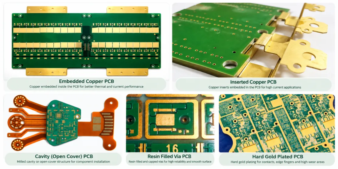
- Resin-filled and plugged through-hole vias
- Capped/planarized vias beneath fine-pitch BGA pads
- Selective backdrilling and controlled-depth via-stub removal
- Fine-pitch BGA escape-routing PCBs
- Special hole diameters, aspect ratios and drill tolerances
For laser vias and build-up sequencing, refer to Highleap’s high-density interconnect production capabilities. Projects with signal-layer via-stub limits can also specify controlled-depth backdrilling.
Flexible and rigid-flex eight-layer constructions
- 8-layer rigid-flex PCB fabrication
- Eight-copper-layer flexible PCB constructions
- Rigid-flex boards with eight layers in rigid areas
- Rigid-flex constructions with different flex-zone layer counts
- Multilayer polyimide flex circuits
- Adhesive and adhesiveless flexible laminate options
- Static-bend and dynamic-bend designs, subject to qualification
- HDI rigid-flex and fine-pitch rigid-flex boards
- Controlled-impedance and RF rigid-flex constructions
- Multiple flexible sections and rigid-to-flex transitions
- Coverlay, selective stiffeners and defined bend windows
- Selective EMI-shielding film in multilayer flex areas, where supported
- Flex assemblies with connector contacts and exposed pads
Highleap’s rigid-flex manufacturing options and multilayer flexible PCB constructions are relevant when identifying the layer count and material system in each zone.
Heavy copper, high-current and thermal features
- 8-layer heavy-copper PCB manufacturing
- Mixed copper weights between signal and power layers
- High-current eight-layer power PCBs
- Heavy-copper inner-layer and outer-layer builds
- Tight-clearance signal layers combined with power planes
- Thermal-via arrays and dense heat-transfer structures
- Embedded copper-coin and copper-inlay constructions, subject to review
- Metal-backed or other special heat-spreading constructions, subject to qualification
- High-voltage isolation and specified creepage/clearance designs
- Thermally demanding multilayer material combinations
For projects combining high-current copper layers with dense signal circuitry, refer to heavy-copper fabrication requirements and specify the copper weight separately for each layer.
Gold fingers, surface finishes and precision machining
- 8-layer PCBs with selective hard-gold fingers
- Long/short and segmented gold-finger contacts
- Stepped, staggered and nonuniform edge-contact arrangements
- Beveled card-edge connectors
- ENIG, ENEPIG and selective finish combinations
- OSP, immersion silver, immersion tin and lead-free HASL finishes
- Board-edge plating and wraparound edge metallization
- Castellated holes and plated half-holes
- Plated slots and non-plated precision slots
- Controlled-depth milling and blind slots
- Stepped pockets, recessed areas and blind cavities
- Special routed openings and internal cutouts
- Counterbored and countersunk mounting holes
- Tight-tolerance press-fit holes
- Edge profiling, V-scoring and routed panel breakaways
- Selective solder-mask opening and via tenting/plugging
- Carbon-ink contacts and special printed conductive features, where supported
- Peelable solder mask and selective solder-mask features, where supported
Contact metallurgy and wear areas should be included in the fabrication notes; hard-gold finger plating is not interchangeable with immersion-gold pad finishes.
Manufacturing confirmation: These are configurations or special processes available for project review, not an unconditional guarantee of every eight-layer combination. Final feasibility, equipment limits, material availability and acceptance requirements are confirmed against the design files before order acceptance.
8 Layer PCB Prototypes, Batch Orders and Volume Manufacturing
Highleap supports eight-layer PCB projects from engineering samples through pilot lots, scheduled releases and repeat production. The practical requirements differ by order stage:
- Prototype and quick-turn: Provide the current revision, the features that must be validated, material constraints and the requested shipment date. Special laminates and sequential processing can affect the schedule.
- Low-volume and pilot runs: Define quantity breaks, inspection evidence, any assembly requirements and changes to the prototype construction before pilot release.
- Batch and high-volume manufacturing: Include the approved stackup, material substitutions policy, panel format, target annual volume, lot acceptance requirements and forecast.
- Repeat orders and supplier transfers: Share the released part number, revision history, critical process approvals and inspection documents needed to keep new lots consistent with the qualified board.
If you need volume manufacturing of an eight-layer rigid-flex, HDI or mixed-dielectric hybrid board, include both the initial order quantity and the recurring demand. Quantity alone does not settle material availability, process yield or lead time; those are checked against the approved build.
Engineering Review for Complex 8-Layer PCB Builds
Before production release, Highleap reviews the fabrication data for the parameters that actually control the job: laminate and bondply grades, the eight copper layers, finished thickness and copper weights; via connections and drilling; board geometry; finishes; and any performance or inspection targets.
- Stackup and electrical sign-off: Confirm the proposed dielectric arrangement, reference layers and impedance targets. Customer approval is required for changes affecting controlled performance. Detailed eight-layer stackup considerations are addressed separately from this manufacturing service.
- Special process sign-off: Identify material mixing, sequential lamination, blind/buried vias, via fill/cap, backdrill limits, controlled-depth features and selective plating.
- Manufacturing data consistency: Ensure Gerber or ODB++ data, drill files, fabrication drawings and the board revision describe the same construction.
- Process exceptions: Where a substitute material, trace compensation or modified feature is proposed, record the exception and obtain approval before fabrication.
Highleap’s pre-production DFM review helps identify missing specifications and manufacturing conflicts before the order is released.
8 Layer PCB Quality and Production Acceptance
Inspection needs to match the agreed product requirements rather than an undefined claim of “high quality.” For eight-layer boards, the production and acceptance plan can cover inner-layer inspection, layer registration, plated-hole integrity, surface finish, final dimensions and bare-board continuity/isolation testing.
Controlled-impedance, RF, HDI or special-reliability orders may additionally specify impedance coupons, microsection results, material identification or traceability reports. Include the required acceptance class, standard revision, sampling or report details in the RFQ so the inspection scope can be priced and agreed. A passed bare-board electrical test alone does not verify insertion loss, flex endurance or every other application-specific requirement.
8 Layer PCB Fabrication and Assembly
Highleap Electronics also supplies assembled eight-layer boards. Projects can be reviewed together for bare PCB manufacturing, component procurement, SMT and through-hole assembly, BGA inspection and specified functional testing through our PCB fabrication and assembly service.
For an assembled HDI, rigid-flex or mixed-material board, panelization, soldering exposure, component placement and test access should be evaluated alongside the bare-board design. Include a BOM with manufacturer part numbers, approved alternates, pick-and-place data, assembly drawings and any firmware or test instructions if PCBA is part of your order.
What to Send for an 8 Layer PCB Manufacturing Quote
Send the most recent manufacturing package, not just “8 layers,” board size and a target price. The following information makes it possible to review the actual scope of your order:
- Gerber or ODB++ fabrication files, NC drill data and the controlled drawing/revision.
- Eight-layer stackup, core/prepreg or bondply schedule, laminate grades and copper weight by layer.
- Board outline, finished thickness, dimensions, tolerances and panel requirements, where specified.
- Via maps, laser-via or backdrill details, filled-via requirements, special cavities and contact plating notes.
- Impedance/loss targets, surface finish and required inspection or measurement reports.
- Prototype, pilot and/or volume quantities, forecast and requested shipment date.
- BOM, placement files, assembly drawings and functional test requirements for PCBA orders.
Request an 8-Layer PCB Manufacturing Quote
Need an eight-layer hybrid-laminate, HDI, rigid-flex, high-speed, heavy-copper or special-process build—prototype or repeat production? Send your files and requirements to Highleap Electronics. We can identify open manufacturing questions and confirm the fabrication and assembly scope for your quotation.
Materials, combined special processes, inspection records and delivery dates are confirmed against the submitted design.

Recommended Posts
5G Small Cell PCB Manufacturing for RF and Telecom Infrastructure
Table of Contents 5G Small Cell PCB Requirements Depend on...
Custom 65% Keyboard PCB and PCBA Manufacturing
Table of contents 1. From Design Files to Production-Ready...
RFSoC Board PCB Manufacturing and Assembly One-Stop Service
Table of contentsReference RFSOC Board Project: 115 × 175...

How to Reduce PCB Costs in 2026
Table of contents Why 80% of PCB Cost Is Locked in at...
How to get a quote for PCBs
Let’s run DFM/DFA analysis for you and get back to you with a report. You can upload your files securely through our website. We require the following information in order to give you a quote:
-
- Gerber, ODB++, or .pcb, spec.
- BOM list if you require assembly
- Quantity
- Turn time
For PCBA services, please provide your BOM (Bill of Materials) and any specific assembly instructions. We also offer DFM/DFA analysis to optimize your designs for manufacturability and assembly, ensuring a smooth production process.