
Peelable Solder Mask Application Process for PCB Manufacturing

Table of Contents
- When Peelable Mask Is Applied in the Process Flow
- Application Methods: Screen Print vs Dispense vs Selective Coat
- Curing Control: Thermal and UV Systems
- Thickness and Edge Definition Control
- Inspection Plan and Peel Test Sampling
- DFM Notes: Marking Peelable Areas on Drawings
- FAQs
When Peelable Mask Is Applied in the Process Flow
Peelable solder mask enters the manufacturing sequence at specific points depending on what it protects and when that protection is needed.
Common Application Points
- Before wave soldering: protects SMT components, connectors, or through-hole areas that should not contact the solder wave
- Before selective soldering: masks keep-out zones adjacent to targeted solder joints
- Before conformal coating: protects connectors, test points, or areas requiring later access
- Before potting or encapsulation: prevents compound from entering specific cavities
- During rework: protects adjacent components during localized reflow or hand soldering
Timing Considerations
The mask must be fully cured before the board enters the thermal process it protects against. For wave soldering, this means application and cure must complete before the board reaches the fluxer. Build schedules should account for cure time plus any queue time before the next operation.
For high-mix environments, peelable mask application often happens at a dedicated station between SMT reflow and wave/selective solder, allowing operators to configure protection based on each assembly’s requirements.
Application Methods: Screen Print vs Dispense vs Selective Coat
Three primary methods exist for applying peelable solder mask, each with distinct advantages depending on volume, geometry, and repeatability requirements.
Screen Printing
Screen printing delivers the most consistent results for production volumes.
Best suited for: High volume production with consistent patterns
Key characteristics:
- Thickness control: Good—controlled by squeegee pressure and mesh count
- Edge definition: Good
- Setup time: Medium—stencil required
- Repeatability: High
Key parameters:
- Mesh count: typically 80-120 mesh for adequate deposit thickness
- Squeegee durometer: 70-80 Shore A for most materials
- Squeegee angle and pressure: affects deposit thickness and edge definition
- Off-contact distance: controls snap-off and print definition
Syringe Dispensing
Manual or semi-automatic dispensing works for low volumes or irregular geometries where stencil costs are not justified.
Best suited for: Prototypes, small runs, complex shapes
Key characteristics:
- Thickness control: Moderate—operator dependent
- Edge definition: Moderate
- Setup time: Low
- Repeatability: Low to Medium
Control factors:
- Needle gauge: affects bead width and flow rate
- Dispense pressure: must match material viscosity
- Operator technique: consistent speed and overlap patterns
Selective Coating Equipment
Automated selective coating systems offer programmable precision for medium-to-high volumes.
Best suited for: Medium to high volume with programmed patterns
Key characteristics:
- Thickness control: Good—programmed parameters
- Edge definition: Very good
- Setup time: Medium—programming required
- Repeatability: High
The equipment deposits material only where needed, reducing waste and improving edge control.
For detailed requirements on integrating peelable mask into your PCB fabrication process, coordinate application method selection with downstream assembly needs.
Curing Control: Thermal and UV Systems
Proper curing determines whether the mask protects effectively and removes cleanly. Both under-cure and over-cure cause problems.
Thermal Cure Systems
Most peelable solder masks cure thermally in convection ovens or inline conveyor systems.
Cure Temperature
- Typical range: 80-150°C (material dependent)
- Under-cure effect: soft mask, poor adhesion
- Over-cure effect: brittle mask, difficult removal
Cure Time
- Typical range: 10-30 minutes (material dependent)
- Under-cure effect: incomplete polymerization
- Over-cure effect: embrittlement
Ramp Rate
- Recommendation: gradual ramp preferred
- Rapid heating effect: may cause bubbles or skinning
UV Cure Systems
Some peelable masks cure under UV exposure, offering faster cycle times.
- Wavelength: typically 365-405nm depending on photoinitiator
- Energy density: specified in mJ/cm², must reach through full thickness
- Shadow areas: UV cannot cure areas blocked by components or board features
Signs of Cure Problems
Under-cure indicators:
- Mask remains tacky after specified cure
- Poor adhesion during handling
- Mask lifts during thermal exposure
- Incomplete protection during soldering
Over-cure indicators:
- Mask becomes hard and brittle
- Tears during removal instead of peeling cleanly
- Leaves residue fragments on board surface
- Difficult to initiate peel edge
Thickness and Edge Definition Control
Consistent thickness ensures adequate protection while enabling clean removal. Edge definition prevents mask from contaminating adjacent solder joints.
Thickness Targets by Application
Wave Solder Protection
- Typical thickness: 200-400 μm
- Considerations: Must withstand solder wave pressure and temperature
Conformal Coat Masking
- Typical thickness: 150-300 μm
- Considerations: Sufficient to prevent coating penetration
Connector Protection
- Typical thickness: 300-500 μm
- Considerations: May need to fill cavities completely
Thickness Measurement Methods
- Wet film gauge: measures immediately after application
- Non-contact optical: measures cured film without damage
- Cross-section (destructive): verification on samples
Edge Definition Control
Poor edge definition allows mask to spread onto solderable areas or leaves gaps in protection.
Control factors:
- Material viscosity (higher viscosity = better edge holding)
- Application method precision
- Time between application and cure (slump potential)
- Board cleanliness affecting wetting behavior
Inspection Plan and Peel Test Sampling
Verification ensures the applied mask will perform as required during soldering and remove cleanly afterward.
Visual Inspection Criteria
- ☐ Complete coverage of specified areas
- ☐ No voids, pinholes, or thin spots
- ☐ Clean edges without bleed onto solderable surfaces
- ☐ No bubbles or contamination in film
- ☐ Uniform color indicating consistent thickness
- ☐ Proper cure (not tacky, not brittle)
Peel Test Sampling Plan
Periodic peel testing verifies the mask will remove properly.
Process Setup
- Sample frequency: First 3 boards
- Test method: Full peel test on coupon or non-critical area
Production Run
- Sample frequency: Every 25-50 boards or hourly
- Test method: Edge lift test + visual
Material Lot Change
- Sample frequency: First 3 boards after change
- Test method: Full peel test
Equipment Parameter Change
- Sample frequency: First 3 boards after change
- Test method: Full peel test
Residue Check
After peel testing, inspect the exposed surface for:
- Visible residue or film remnants
- Surface discoloration
- Contamination that could affect solderability
For PCB assembly services requiring peelable mask, establish inspection criteria during process qualification to ensure consistent quality.
DFM Notes: Marking Peelable Areas on Drawings
Clear documentation prevents misapplication and ensures repeatability across production lots and manufacturing partners.
What to Include in Fab/Assembly Drawings
- Area definition: clearly bounded regions requiring peelable mask
- Keep-out zones: minimum clearance from solderable features
- Thickness requirement: target range with tolerances
- Material specification: if specific material is required
- Cure requirements: if specific cure method is mandated
- Inspection requirements: acceptance criteria and sampling
Gerber Layer Convention
Define peelable mask areas on a dedicated Gerber layer:
- Use positive image showing mask coverage areas
- Include edge clearances in the artwork
- Note layer purpose clearly in file naming and readme
Drawing Note Example
“Apply peelable solder mask to areas indicated on layer [X]. Target thickness: 250-350 μm. Thermal cure per material specification. Maintain minimum 0.5mm clearance from all solderable surfaces. Mask shall peel cleanly without residue after wave soldering exposure.”
For comprehensive guidance on peel off solder mask materials and selection, coordinate application process parameters with material-specific recommendations.
FAQs
1. How thick should peelable solder mask be for wave soldering?
Typical thickness for wave solder protection ranges from 200-400 μm. The mask must be thick enough to withstand solder wave pressure and thermal exposure without breakthrough, but not so thick that it becomes difficult to remove cleanly.
2. Can peelable mask be applied over components?
Yes, peelable mask can cover and protect components during subsequent soldering operations. Ensure the mask material is compatible with component materials and that removal will not damage the components.
3. How long after application should curing begin?
Cure promptly after application to prevent slump, contamination, or skinning. Most processes cure within 30 minutes of application. Check material data sheet for specific open time limits.
4. What causes bubbles in peelable mask?
Bubbles typically result from trapped air during application, outgassing from the board surface, or too-rapid heating during cure. Ensure clean, dry boards and gradual thermal ramp during cure.
5. How do I verify the mask will peel cleanly before production?
Conduct peel tests on sample boards processed through the actual cure profile. Test adhesion after simulated or actual thermal exposure (wave solder equivalent). The mask should lift cleanly with no residue and no damage to the board surface.

Recommended Posts

RF Transceiver PCB Manufacturing and Assembly
Table of contentsRF Transceiver PCB Manufacturing and...
RFSoC Board PCB Manufacturing and Assembly One-Stop Service
Highleap Electronics supports customer-designed RFSOC...
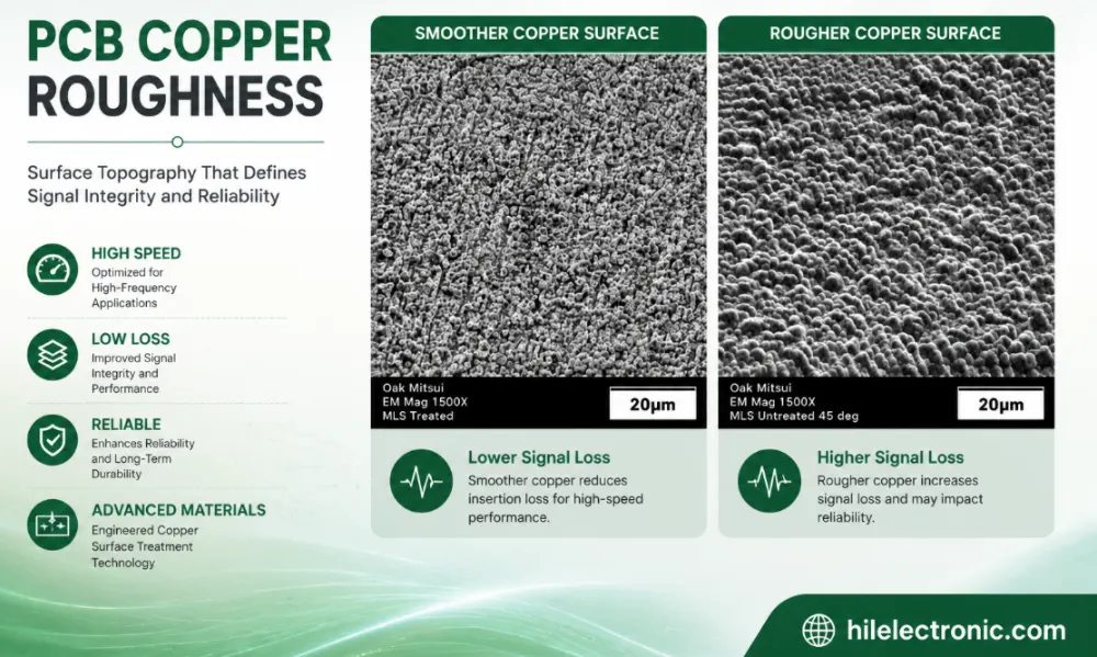
PCB Copper Roughness: Signal Loss, Material Selection and Manufacturing Control
Table of contentsWhat Is PCB Copper Roughness?How Copper...

800G Optical Module PCB Manufacturing and Assembly Service
Table of contentsWhat Makes an 800G Optical Module PCB...
How to get a quote for PCBs
Let us run DFM/DFA analysis for you and get back to you with a report.
You can upload your files securely through our website.
We require the following information in order to give you a quote:
-
- Gerber, ODB++, or .pcb, spec.
- BOM list if you require assembly
- Quantity
- Turn time
In addition to PCB manufacturing, we offer a comprehensive range of electronic services, including PCB design, PCBA (Printed Circuit Board Assembly), and turnkey solutions. Whether you need help with prototyping, design verification, component sourcing, or mass production, we provide end-to-end support to ensure your project’s success. For PCBA services, please provide your BOM (Bill of Materials) and any specific assembly instructions. We also offer DFM/DFA analysis to optimize your designs for manufacturability and assembly, ensuring a smooth production process.