
PoE Switch PCB Manufacturing for Power over Ethernet Network Hardware
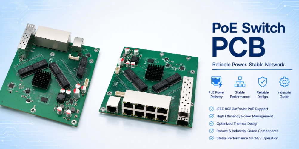
Table of Contents
- PoE Switch PCB Architecture: Where Power and Ethernet Share the Same Board
- Copper, Current Paths, and Thermal Design for PoE Power Delivery
- Protecting Ethernet Signal Integrity Around PoE Power Circuits
- Surge, ESD, Isolation, and Port-Side Layout Considerations
- PoE Switch PCB Fabrication and Assembly Controls That Matter
- Testing a PoE Switch PCBA Without Confusing PCB Quality With Product Certification
- RFQ Checklist for PoE Switch PCB Manufacturing and Assembly
A PoE switch PCB has to do two jobs at the same time: route Ethernet data with controlled electrical behavior and distribute DC power to powered devices through the Ethernet cabling interface. That combination changes the board from a conventional digital switch platform into a mixed high-speed, power, thermal, and protection design. For buyers and hardware teams, the manufacturing question is therefore not simply whether a factory can build a multilayer PCB. The more useful question is whether the fabrication and assembly process can preserve the stackup, impedance, copper geometry, isolation spacing, component placement, and thermal details that the PoE design depends on. Highleap Electronics supports communication PCB manufacturing and turnkey PCB assembly from prototype through production, with engineering review based on the customer-approved design data and test requirements.
1. PoE Switch PCB Architecture: Where Power and Ethernet Share the Same Board
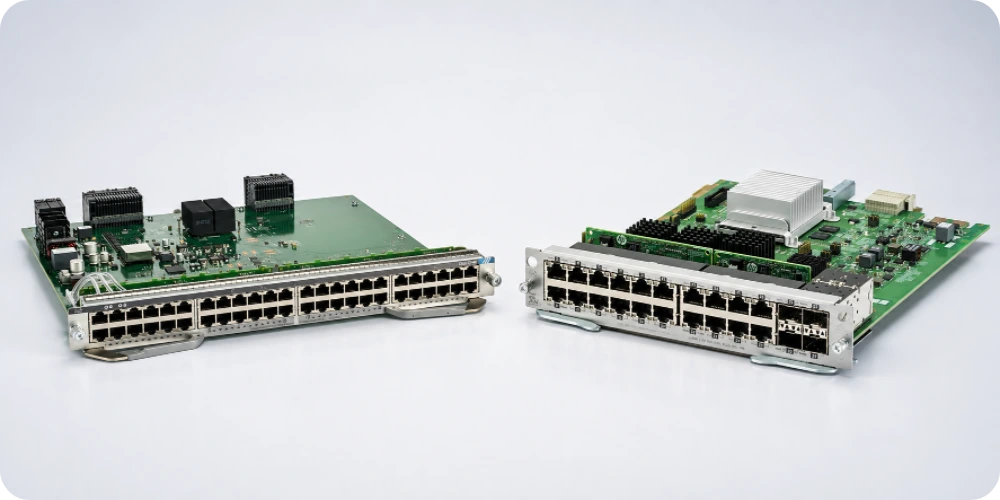
A PoE Ethernet switch normally combines several functional zones: the switch processor or switching ASIC, Ethernet PHY devices, memory and management circuitry, port-side magnetics and connectors, PoE power-sourcing circuitry, DC/DC conversion, protection devices, and system power input. The exact architecture varies by port count, Ethernet speed, PoE type, thermal budget, and enclosure design.
1.1 IEEE 802.3 PoE Changes the Power Path, Not the Basic Ethernet Requirement
Power over Ethernet is standardized within IEEE 802.3. Earlier PoE implementations use the two-pair approaches associated with IEEE 802.3af and 802.3at, while IEEE 802.3bt extends standardized PoE to four-pair power delivery and higher available power. For PCB manufacturing, that distinction matters because higher power increases current density, copper-loss sensitivity, heat generation, and the importance of port-to-port consistency.
The PCB manufacturer should not redesign the PoE classification or detection circuit. Those functions are defined by the customer’s schematic and the selected PSE controller. Manufacturing must instead preserve the intended copper paths, component footprints, isolation barriers, and connector/magnetics interface.
1.2 Separate the Board Into Electrical Zones Before DFM
A useful DFM review begins by understanding which regions are electrically sensitive:
- High-speed data zone: switch-to-PHY interfaces, PHY-to-magnetics differential routing, reference planes, clocks, and management buses.
- PoE power zone: PSE controllers, MOSFETs, current-sense elements, bulk decoupling, DC/DC converters, and high-current copper distribution.
- Port protection zone: TVS devices, common-mode components where specified, magnetics, RJ45 connectors, and chassis/earth referencing according to the system design.
- Thermal zone: switching devices, regulators, PSE circuitry, and other components whose heat must be transferred into copper, thermal vias, heatsinks, or the enclosure.
Keeping those functions physically understandable on the PCB helps both the hardware team and the manufacturer identify risks before production. For complex layer structures, a documented PCB stackup is more useful than a generic request such as “multilayer FR-4.”
| RFQ Input | Why It Changes Manufacturing | What the Factory Needs |
|---|---|---|
| PoE architecture / power budget | Changes current density, heat, power-device selection and port loading assumptions. | Approved schematic context, PSE controller, simultaneous powered-port assumptions and thermal limits. |
| Layer stackup and copper by layer | Controls impedance geometry, current carrying paths, etch compensation and finished thickness. | Released stackup, copper weights, finished thickness and controlled-impedance list. |
| Magnetics / RJ45 implementation | Affects breakout routing, isolation region, through-hole process and sourcing risk. | Exact approved part numbers, land patterns and substitution rules. |
| Transient / isolation requirements | Determines keep-outs, slots, spacing and protection-component placement that must not be altered. | Dimensioned fabrication notes and product-level constraints. |
| PCBA test scope | Determines test-point access, fixtures, loads, programming and cycle time. | Test procedure, software, fixtures, loads and pass/fail limits. |
2. Copper, Current Paths, and Thermal Design for PoE Power Delivery
The PoE section is often the part of the switch board where a layout that looks electrically correct can still become difficult to manufacture reliably. Copper thickness, finished trace geometry, plane neck-downs, via current sharing, and local heat spreading all interact.
2.1 How Should Copper Weight Be Chosen for a PoE Switch PCB?
There is no single “correct copper weight” for a PoE switch PCB. The required copper should be checked against current path geometry and allowable temperature rise rather than selected from port count alone; our PCB trace current-capacity resource explains the manufacturing variables that affect this decision. A 24-port switch does not automatically require a particular ounce value. The correct construction depends on the current carried by each segment, allowable temperature rise, copper width, copper thickness, layer placement, ambient temperature, airflow, connector limitations, and how many ports can deliver power simultaneously.
For fabrication, the important step is to freeze the copper requirement early. Increasing copper thickness late in the project can change etching compensation, minimum spacing, controlled-impedance geometry, press thickness, and even the manufacturability of fine-pitch digital areas. If the board combines fine-pitch BGA routing with heavier power copper, the stackup may need different copper weights on different layers rather than one heavy-copper rule everywhere.
2.2 Thermal Vias Are Useful Only When They Connect to a Real Heat Path
Via arrays under exposed pads, MOSFETs, regulators, and PoE controllers can conduct heat into internal or opposite-side copper. But a dense via field does not guarantee good thermal performance if it terminates in small isolated copper areas or is blocked by the mechanical design. The PCB drawing should therefore define via type and filling requirements where solder wicking or via-in-pad assembly is a concern.
For higher-density power designs, Highleap can review manufacturability together with thermal features described in the design package. Related methods such as copper spreading, thermal via structures, and heavier copper are discussed in our PCB thermal management resource.
2.3 Current-Sense Paths Require Geometry Consistency
Many PSE implementations measure current through dedicated sense resistors or controller-defined sensing structures. The PCB manufacturer should preserve Kelvin connections and the intended copper geometry around these circuits. Casual CAM edits near the sense path can change parasitic resistance or measurement behavior. These features should be identified as electrically critical during DFM review so routine manufacturability adjustments do not disturb them.
3. Protecting Ethernet Signal Integrity Around PoE Power Circuits
PoE does not remove the signal-integrity requirements of Ethernet. The data path still depends on the PHY implementation, controlled differential routing, reference continuity, connector/magnetics layout, and the device vendor’s placement guidance.
3.1 Controlled Impedance Is a Stackup-and-Geometry Requirement
Ethernet differential pairs should be manufactured to the impedance target defined in the design documentation. The PCB factory should not assume that every differential pair on the board is the same impedance. Switch-to-PHY SerDes, PHY-to-magnetics traces, clocks, and other high-speed interfaces may have different requirements.
The best production package identifies each controlled structure, its reference plane, the target impedance, and the allowed tolerance. Highleap’s high-speed PCB manufacturing work includes stackup and impedance considerations for data-networking hardware.
3.2 Avoid Power-Conversion Noise Coupling Into Sensitive Routing
The PSE and DC/DC sections can contain fast switching edges and high di/dt current loops. Those loops should remain compact and should not share poorly controlled return paths with sensitive clocks or high-speed pairs. From a manufacturing perspective, the key requirement is to preserve the customer’s plane segmentation, stitching-via pattern, copper keep-outs, and component placement rather than “cleaning up” the layout visually.
3.3 Pair Symmetry Matters Through the Port Interface
At the port side, differential routing should maintain pair symmetry and minimize unnecessary discontinuities. Magnetics may be integrated into the connector or implemented as separate components. In either case, pad geometry, pair breakout, and component orientation should follow the approved layout. If substitutions are proposed during sourcing, the replacement part must be checked for footprint, pinout, electrical function, temperature rating, and any magnetics or PoE-specific characteristics before assembly.
Highleap Electronics • PCB Manufacturing & PCBA
Review Your PoE Switch PCB Project
Send the PoE power budget, Ethernet interface requirements, stackup, BOM, thermal targets and production test plan for PCB and PCBA review.
4. Surge, ESD, Isolation, and Port-Side Layout Considerations
Network ports connect the switch PCB to long external cables, so the port region deserves different treatment from an internal digital interface. Protection strategy depends on the product’s target standards, installation category, grounding arrangement, enclosure, and end-market requirements.
4.1 Protection Components Need Short, Intentional Current Paths
TVS diodes and other transient-protection components are only effective when the surge current can flow through a controlled low-inductance path. Long traces between connector, protection device, and the intended return node reduce effectiveness. The manufacturer should preserve these paths and avoid unnecessary neck-downs introduced by panel or tooling edits.
4.2 How Much Creepage and Clearance Does a PoE Switch PCB Need?
Ethernet magnetics provide galvanic isolation in standard Ethernet implementations, but there is no universal PCB creepage or clearance value that applies to every PoE switch. The required spacing depends on the product safety architecture, working voltages, environment, applicable standards, enclosure and insulation system. The system designer must therefore define the required distances and isolation features. For boards exposed to cable-side transients, the broader EMI/EMC PCB design context should also be considered at product level. The PCB drawing should explicitly mark any isolation slots, copper keep-outs, restricted via areas, or minimum spacing that must not be altered. If the finished switch is intended for a specific safety or EMC regime, those requirements should be translated into measurable PCB and assembly instructions rather than left as a general “industrial grade” note.
4.3 Chassis and Signal Ground Should Not Be Merged by Assumption
Some switch designs use separate chassis and digital ground regions with controlled coupling; others implement different grounding approaches. The PCB manufacturer should follow the customer-approved design and must not bridge ground regions to improve copper balance unless the engineering team approves the change. Copper balancing should be solved without changing electrical intent.
5. PoE Switch PCB Fabrication and Assembly Controls That Matter
A PoE switch PCBA can combine large connectors, fine-pitch ICs, power packages, magnetics, and high-current structures on one board. That mixture requires coordinated fabrication and assembly planning. Highleap can combine PCB fabrication, component sourcing, SMT/THT assembly, AOI/X-ray inspection, and customer-defined functional testing within one project flow; the exact inspection and test scope is confirmed against the approved build package.
5.1 Fabrication Review
Before production, the PCB data should be checked for layer registration, copper-to-edge clearance, drill aspect ratio, solder-mask dams, annular rings, via structures, copper balance, controlled-impedance geometry, and any special isolation features. The final surface finish should match the component, connector, shelf-life, and assembly requirements rather than being selected solely by habit.
5.2 Assembly Planning
The BOM should identify exact manufacturer part numbers and approved alternates. Ethernet transformers, integrated-magnetics connectors, PSE controllers, power MOSFETs, sense resistors, oscillators, and high-speed PHY devices are not good candidates for uncontrolled substitution.
For hidden solder joints such as BGA or certain QFN/LGA packages, X-ray inspection can complement AOI because AOI cannot see joints under the package body. Through-hole RJ45 connectors, power connectors, or transformers may require selective soldering, wave soldering, or manual processes depending on the assembly design. Highleap’s SMT assembly service can be combined with through-hole and inspection steps specified for the project.
5.3 Prototype and Production Builds Have Different Learning Goals
Prototype builds should verify fit, assembly process, power behavior, thermal hot spots, port operation, and test access. Production then depends on controlling approved materials, component revisions, stackup, process changes, and test criteria. A prototype PCB build is most valuable when the results are fed back into the production release instead of treating prototype and volume data as separate projects.
6. Testing a PoE Switch PCBA Without Confusing PCB Quality With Product Certification
PCB manufacturing tests verify the board and assembly against defined manufacturing requirements. They do not by themselves certify that the finished network product complies with IEEE 802.3, safety standards, EMC requirements, or regional regulatory rules.
6.1 Bare-Board Verification
Typical bare-board controls can include electrical continuity/isolation testing, dimensional inspection, solder-mask and surface-finish inspection, and controlled-impedance coupon measurement when impedance is specified. Microsection analysis may be requested for multilayer via structures, higher-reliability builds, or customer-defined quality plans.
6.2 Assembly Inspection
Assembly inspection may combine solder-paste inspection, AOI, X-ray for hidden joints, visual inspection, polarity/orientation checks, and workmanship criteria. The appropriate inspection route depends on package types and the agreed quality plan.
6.3 Can a PCB Manufacturer Certify IEEE 802.3 PoE Compliance?
No routine bare-board or PCBA inspection by itself certifies a finished product to IEEE 802.3. A useful functional test for a PoE switch may check boot, management access, Ethernet link establishment, port-to-port traffic, PoE detection/classification behavior, power delivery under defined loads, current monitoring, and thermal behavior. However, these tests require a fixture, test software, limits, loads, and pass/fail criteria. Highleap can manufacture and assemble to the supplied test specification; final product compliance remains tied to the complete device design and the applicable certification program.
7. RFQ Checklist for PoE Switch PCB Manufacturing and Assembly
For an accurate PoE switch PCB or turnkey PCBA quotation, send enough information for both fabrication and assembly review. A useful package includes:
- Gerber RS-274X, Gerber X2, or ODB++ production data
- Excellon drill files and fabrication drawing
- Approved layer stackup, finished thickness, and copper weight by layer
- Controlled-impedance targets and tolerances
- PoE type or power architecture relevant to the design review
- Isolation slots, keep-outs, creepage/clearance notes, and any special safety constraints
- BOM with manufacturer part numbers and approved substitution rules
- Pick-and-place file and assembly drawing
- Programming requirements for MCU, EEPROM, CPLD, or other programmable devices
- PCBA test procedure, fixtures, test software, and pass/fail limits if functional testing is required
- Prototype and production quantities plus packaging/traceability requirements
Highleap Electronics can review the complete data package for PCB fabrication, component sourcing, assembly, and testing preparation. The most reliable quote is based on the actual stackup, BOM, power architecture, quality plan, and test scope—not only the number of layers and ports. For switch-specific production validation, see our network switch PCB reliability testing guide.

Recommended Posts

Isola Astra MT77 PCB Manufacturing
Figure 1. Isola Astra MT77 PCB ManufacturingIsola Astra...

Nelco N4000-13 PCB Material and Manufacturing Guide | Highleap Electronics
Figure 1. Nelco N4000-13 PCBNelco N4000-13 PCB is a...

Copper Clad Laminate: Complete Material Selection Guide for PCB Engineers
Every electrical property that matters in a printed...

Inside a China Ceramic PCB Factory: Process Control Across Power/LED/RF/Medical
Table of Contents Inside a China Ceramic PCB Factory: How...
How to get a quote for PCBs
Let’s run DFM/DFA analysis for you and get back to you with a report. You can upload your files securely through our website. We require the following information in order to give you a quote:
-
- Gerber, ODB++, or .pcb, spec.
- BOM list if you require assembly
- Quantity
- Turn time
For PCBA services, please provide your BOM (Bill of Materials) and any specific assembly instructions. We also offer DFM/DFA analysis to optimize your designs for manufacturability and assembly, ensuring a smooth production process.