
Ethernet Switch PCB Manufacturing for High-Speed Networking Hardware
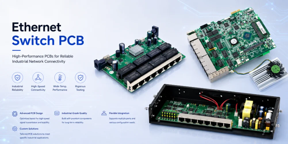
Table of Contents
- Start With the Switch Architecture, Not a Generic “Ethernet PCB” Specification
- PCB Stackup and Controlled Impedance for Switch-to-PHY and Port-Side Routing
- Via Structures, Connectors, and Loss Budget in Gigabit and Multi-Gigabit Switch Hardware
- Power Distribution, Clocks, and Return-Path Control on Ethernet Switch Boards
- PCB Assembly for Switch ASICs, PHYs, Magnetics, RJ45, and Pluggable Interfaces
- Inspection and Functional Test Strategy for Ethernet Switch PCBAs
- Engineering Package Checklist: From Prototype Ethernet Switch PCB to Production
An Ethernet switch PCB is a manufacturing platform for several different electrical domains: a switching device or processor, Ethernet PHYs, memory, clocking, power conversion, management circuitry, and copper or optical port interfaces. The board may support only a few copper ports or combine many ports with SFP/SFP+/other pluggable interfaces. Because the electrical requirements change with architecture and data rate, a useful manufacturing plan starts from the actual schematic, stackup, channel constraints, and assembly BOM—not from a generic “network switch PCB” specification. Highleap Electronics provides high-speed communication PCB manufacturing and turnkey PCBA support for networking hardware, including controlled-impedance multilayer boards, dense assembly, and production-oriented engineering review.
1. Start With the Switch Architecture, Not a Generic “Ethernet PCB” Specification
The same product category can contain very different PCB challenges. A compact unmanaged switch may use a highly integrated switch/PHY device and several magnetics modules. A managed platform may add a separate CPU, DDR memory, flash, multiple PHYs, SFP cages, redundant power, console ports, and a large switching ASIC.
1.1 Identify Every High-Speed Interface Before Stackup Release
The design team should mark the interfaces whose electrical behavior depends on controlled geometry. These can include PHY-to-magnetics differential pairs, serial interfaces between a switch ASIC and PHYs, high-speed memory buses, clock lines, PCIe or other host interfaces on more complex platforms, and high-speed connections to optical modules.
Not every net needs impedance control. Treating every route as “high speed” increases cost without adding performance. The fabrication drawing should identify the structures that actually require controlled impedance and the tolerance expected for each one.
1.2 Copper Ports and Optical Ports Create Different Layout Constraints
Copper Ethernet ports route through magnetics and external connectors. Pluggable optical/electrical modules can involve high-speed serial channels, cage mechanics, connector launch geometry, and longer loss-sensitive paths. If both are present, the board may need different routing rules in different regions.
1.3 Port Count Drives More Than Board Size
As port count increases, the design may require more PHY channels, power rails, clock distribution, I/O connectors, thermal spreading, and dense escape routing. This can push the design toward higher layer count or HDI PCB features. The manufacturing goal is to add complexity only where it solves a routing or signal-integrity constraint.
| Switch Interface / Feature | Typical PCB Concern | Manufacturing Information to Freeze |
|---|---|---|
| PHY-to-magnetics / copper ports | Pair geometry, reference continuity, isolation region and connector breakout. | Impedance targets, magnetics/RJ45 part numbers, keep-outs and mechanical tolerances. |
| Switch-to-PHY high-speed interface | Loss, skew, return-path continuity and via transitions. | Interface type, controlled nets, reference layers, stackup and any length/skew limits. |
| SFP/SFP+/QSFP-family interfaces | Connector launch, cage mechanics and potentially tighter loss budgets. | Approved connector/cage data, board-edge geometry and channel constraints. |
| BGA switch ASIC / memory | Escape density, via structure, warpage and hidden solder joints. | Package data, via-in-pad/HDI requirements, stencil plan and X-ray criteria. |
| Power rails / clocks | PDN noise, thermal concentration and clock sensitivity. | Power architecture, critical clocks, thermal interface and test points. |
2. PCB Stackup and Controlled Impedance for Switch-to-PHY and Port-Side Routing
The stackup is one of the earliest manufacturing decisions that can materially change Ethernet switch performance. Dielectric thickness, copper thickness, resin content, glass style, reference-plane placement, and final trace geometry all influence impedance and loss.
2.1 Build the Stackup Around Reference Planes
High-speed layers should have continuous reference planes placed at controlled distances. This gives the layout team predictable impedance and short return-current paths. Power and ground layer placement also affects power-distribution impedance and crosstalk between routing layers.
For manufacturing, the approved PCB stackup specification should identify laminate family, core/prepreg structure, copper weights, finished thickness, and controlled-impedance layers. If a supplier proposes an equivalent dielectric construction, the change should be reviewed electrically before release.
2.2 Does Every Ethernet Switch PCB Need Low-Loss Material?
No. Well-designed FR-4 systems are appropriate for many Ethernet switch channels when the loss budget and construction allow it. Lower-loss laminates become useful when edge rate, channel length, connector launches, serial data rate, or insertion-loss margin makes standard material inadequate. The correct decision comes from the channel budget; our high-speed PCB material selection guide explains the manufacturing variables that should be compared instead of treating a laminate brand as a performance guarantee.
Highleap works with standard and lower-loss material families used in high-speed PCB manufacturing. Material substitutions should be evaluated for Dk, Df, thickness availability, copper profile, thermal behavior, and lamination compatibility.
2.3 Impedance Coupons Verify the Fabricated Structure
When controlled impedance is required, test coupons can be placed on the production panel and measured after fabrication. A coupon verifies the manufactured stackup and geometry; it does not replace end-to-end channel validation on the assembled system. The test requirement, target, tolerance, reference layer, and coupon structures should be part of the order documentation.
3. Via Structures, Connectors, and Loss Budget in Gigabit and Multi-Gigabit Switch Hardware
Discontinuities become increasingly important as signal edge rates and channel frequencies rise. Vias, connector launches, stubs, layer transitions, and reference-plane changes all add parasitic effects.
3.1 Does an Ethernet Switch PCB Always Need Back Drilling?
No. A standard plated through via can be perfectly acceptable when the channel budget allows it. PCB back drilling, blind vias, or microvias are introduced when unused via stubs or routing density become significant enough to justify the added process. The manufacturer should receive the controlled-depth drilling table or HDI build sequence rather than infer the intent from Gerber files.
3.2 Connector Launch Geometry Must Stay Consistent
RJ45 magnetics, board-to-board connectors, mezzanine connectors, and pluggable-module sockets each create a transition between structures. Pad size, antipad geometry, reference-via placement, and breakout routing can dominate the local impedance. Fabrication CAM changes near these launches should be minimized and reviewed when required.
3.3 Do Not Ignore Mechanical Tolerances Around Cages and Connectors
SFP-family cages, stacked RJ45 connectors, LEDs, light pipes, and enclosure cutouts create tight mechanical relationships. Board outline tolerance, connector position, mounting-hole location, and solder joint seating can affect final fit. A 3D model or mechanical drawing helps the assembler identify interference before production.
Highleap Electronics • PCB Manufacturing & PCBA
Review Your Ethernet Switch PCB Project
Send the released stackup, high-speed interface requirements, BOM and mechanical details for fabrication and assembly review.
4. Power Distribution, Clocks, and Return-Path Control on Ethernet Switch Boards
The signal path gets most of the attention, but many switch failures begin with power integrity, clock quality, or return-path problems.
4.1 Switching Devices Often Need Multiple Low-Voltage Rails
Switch ASICs and processors may use separate core, I/O, memory, analog, and SerDes supplies. The regulator topology and sequence are device-specific. On the PCB, broad power planes, local decoupling, via placement, and low-impedance connections help the power-distribution network behave as intended.
4.2 Clock Routing Should Be Treated as an Electrical Interface
Reference oscillators and clocks for PHYs or switch devices can be sensitive to noise and return discontinuities. The manufacturer should preserve guard/keep-out structures and avoid moving stitching vias or reference copper around these circuits unless approved.
4.3 Return-Path Discontinuities Can Be Worse Than Trace-Length Differences
A differential pair crossing a split plane or changing reference without adequate stitching can produce common-mode noise and EMI. This cannot be fixed by fabrication after the layout is released. A practical DFM review can flag plane breaks, manufacturability issues, and via constraints, while final signal-integrity validation remains part of the hardware design process.
5. PCB Assembly for Switch ASICs, PHYs, Magnetics, RJ45, and Pluggable Interfaces
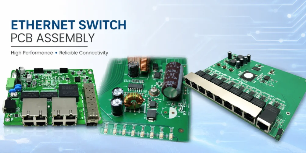
Ethernet switch PCBA is often a mixed-technology build. Fine-pitch BGA assembly may sit beside QFNs, crystals, power inductors, large RJ45 connectors, press-fit or through-hole parts, and metal cages.
5.1 BGA and QFN Assembly Needs Package-Specific Process Control
Stencil design, paste volume, reflow profile, board support, and package moisture handling influence joint quality. Via-in-pad under BGA or QFN thermal pads should have the correct fill/cap specification where open vias would wick solder. X-ray is useful for hidden joints and thermal-pad void assessment because these features cannot be fully evaluated by AOI.
5.2 Magnetics and Ethernet Connectors Need Controlled Substitution
Two RJ45 connectors that look mechanically similar may use different integrated magnetics, LED pinouts, center-tap arrangements, shield construction, or PoE capability. Likewise, discrete magnetics modules have electrical specifications that must match the design. BOM substitution should therefore be approved by engineering, not based on footprint alone.
5.3 Large Connectors Affect the Soldering Route
Depending on the connector design and board mix, through-hole parts may be wave soldered, selectively soldered, or manually soldered after SMT. Thermal relief, hole size, copper connection, and keep-out around neighboring components should be compatible with the chosen process. Highleap’s SMT PCB assembly service can be integrated with through-hole assembly for complete switch PCBAs.
6. Inspection and Functional Test Strategy for Ethernet Switch PCBAs
A good test plan separates manufacturing defects from system-level Ethernet performance.
6.1 Bare Board
100% electrical continuity/isolation testing is a normal starting point for fabricated boards. Impedance coupons are added when controlled impedance is specified. Dimensional, solder-mask, finish, drill, and visual inspection confirm that the physical board matches the released requirements.
6.2 Assembly Inspection
SPI can check solder-paste deposition before placement. AOI checks component presence, polarity, alignment, and visible solder joints. X-ray inspection is added for BGA, LGA, QFN, or other hidden solder interfaces. These methods complement one another; none alone proves that an Ethernet port functions correctly.
6.3 What Should Ethernet Switch PCBA Functional Testing Cover?
Functional testing can include power rails, current consumption, boot sequence, programming, management interface, port link-up, loopback or traffic testing, LED operation, and optical-module recognition where applicable. Test depth depends on the fixture and software supplied or jointly developed for the project. PCB/PCBA inspection does not replace IEEE 802.3 interoperability, EMC, safety, or regulatory qualification of the finished switch.
7. Engineering Package Checklist: From Prototype Ethernet Switch PCB to Production
For an accurate quotation and a controlled production release, include:
- Gerber/ODB++ data and drill files
- Fabrication drawing with board dimensions, tolerances, and special processes
- Approved stackup and material requirements
- Controlled-impedance list with target, tolerance, and reference layer
- BOM with approved manufacturer part numbers and alternate policy
- Pick-and-place data and assembly drawings
- Connector/cage mechanical details for critical interfaces
- Programming files and instructions
- Functional-test procedure, software, fixtures, and pass/fail limits
- Prototype, pilot, and production quantities plus traceability requirements
A staged PCB prototype build is useful for validating the stackup, mechanical fit, assembly process, thermal behavior, and test method before the production data set is frozen. Highleap Electronics can support fabrication-only, consigned assembly, or turnkey PCB assembly according to the sourcing and test scope defined by your team. For related switch architecture and verification topics, see our switch PCB overview and network switch PCB reliability testing guide.

Recommended Posts

TMM4 Filter PCB Manufacturing
TMM4 filter PCB manufacturing is controlled by the...

TMM3 PCB Manufacturing for RF Modules
TMM3 PCB manufacturing is most useful where the RF module...

TMM6 PCB Fabrication
TMM6 fabrication is the process-control page for a mid-Dk...
TMM13i PCB Manufacturing
TMM13i PCB manufacturing is aimed at ultra-compact RF...
How to get a quote for PCBs
Let’s run DFM/DFA analysis for you and get back to you with a report. You can upload your files securely through our website. We require the following information in order to give you a quote:
-
- Gerber, ODB++, or .pcb, spec.
- BOM list if you require assembly
- Quantity
- Turn time
For PCBA services, please provide your BOM (Bill of Materials) and any specific assembly instructions. We also offer DFM/DFA analysis to optimize your designs for manufacturability and assembly, ensuring a smooth production process.