
FR408HR PCB Stackup, Impedance, Dk/Df and TDR
An FR408HR PCB stackup is an electrical and manufacturing model, not a decorative layer diagram. It connects controlled-impedance targets to real core constructions, prepreg glass styles, resin content, pressed thickness, copper foil, finished copper, solder mask, lamination behavior and production tolerance.
This guide focuses on how FR408HR constructions are modeled for impedance, insertion loss, coupon planning, and fabrication release. For supplier selection and quotation requirements, review the FR408HR PCB manufacturer and material guide.
FR408HR Properties Used in Stackup Design
Stackup work should begin by separating published laminate data from the effective electrical behavior of the selected construction. Dk and Df depend on test method, frequency, resin content, glass style and the way the finished board is built.
For background on how laminate Dk is interpreted in transmission-line calculations, review the PCB dielectric constant guide before selecting a solver value.
Electrical Property Snapshot
The general Isola data sheet publishes frequency-dependent Dk and Df values, while a separate construction table provides values by core/prepreg glass style, resin content, thickness and frequency. The general values below are useful for orientation only. A production model should select data that matches the actual construction and the field-solver methodology.
| Frequency | General typical Dk | General typical Df | Modeling note |
|---|---|---|---|
| 100 MHz | 3.72 | 0.0072 | Do not mix this test result with higher-frequency construction data without documenting the method. |
| 1 GHz | 3.69 | 0.0091 | Useful as a general reference; glass style and resin content still shift the effective value. |
| 2 GHz | 3.68 | 0.0092 | This is the widely quoted pair, but it is not a universal finished-board Dk/Df. |
| 5 GHz | 3.64 | 0.0098 | Conductor roughness and launch/via loss may become as important as the dielectric term. |
| 10 GHz | 3.65 | 0.0095 | Use construction-specific data and validate the complete channel where loss margin is limited. |
Important: core and prepreg constructions in the Isola Dk/Df tables span a meaningful range. Resin percentage, glass weave, pressed thickness, copper roughness, solder mask and local resin distribution change the effective electrical behavior. The released stackup should record the value and method used in the model.
What the Data Sheet Can—and Cannot—Predict
The general Isola data sheet lists typical thermal and electrical properties for the material family. It is useful for early material selection. The construction-specific Dk/Df tables go further by listing dielectric behavior for individual core and prepreg glass/resin combinations from 100 MHz through 10 GHz.
A single Dk value is not the whole material model
The widely repeated Dk 3.68 and Df 0.0092 correspond to typical 2 GHz values in the general data table. Individual constructions can be higher or lower because glass has a different dielectric behavior from resin, and the resin percentage varies. Frequency and test method also matter. The design team should therefore document which value was used for pre-layout simulation and allow the manufacturer to update the final impedance model from the selected construction.
Prepreg values require particular care
Prepreg is not a fixed-thickness sheet after lamination. Its final thickness depends on glass style, resin content, copper topography, pressure, flow, and cure. A prepreg table provides a nominal construction reference, not a guaranteed dielectric gap in every board. The fabricator’s pressed-thickness model should be used for the released stackup.
Spread-weave glass reduces—but does not eliminate—glass effects
The updated FR408HR Dk/Df table notes that the glass is spread weave in both directions. This helps produce a more uniform glass distribution than conventional open weave, but trace location, angle, width, and local resin/glass composition can still matter in tightly matched differential channels.
Copper foil is part of the electrical model
Isola lists reverse-treated foil as a standard offering, with other foil options available. Copper profile affects conductor loss and effective geometry. For a loss-sensitive design, the stackup should identify foil type or roughness assumptions rather than treating all one-ounce copper as electrically identical.
Information Required Before Stackup Modeling
The layer count and finished thickness are not enough. The fabricator needs conductor geometry, copper weights, signal types, impedance targets, reference planes, loss constraints, via architecture, assembly exposure and mechanical limits before a useful production stackup can be proposed.
Start From Product Requirements
Before selecting cores and prepregs, define the constraints the stackup must satisfy. These constraints often conflict, so the design team should identify priority.
Electrical
Impedance, insertion loss, crosstalk, propagation delay, reference-plane continuity, power-distribution impedance, and isolation.
Mechanical
Finished thickness, connector fit, press-fit hole, board stiffness, bow/twist, enclosure clearance, and controlled-depth features.
Manufacturing
Available constructions, copper balance, resin demand, lamination cycles, drill aspect ratio, registration, and panel yield.
Assembly
BGA escape, via-in-pad, component coplanarity, reflow exposure, panel support, depaneling, and thermal mass.
Reliability
PTH fatigue, CAF spacing, moisture, thermal cycling, sequential lamination, field environment, and product life.
Commercial
Material availability, standard sheet utilization, prototype-to-production continuity, cost, lead time, and approved suppliers.
A thin dielectric may make a target impedance easier with a narrow trace but can increase plane capacitance and manufacturing sensitivity. A thick dielectric may improve isolation but require a wider trace or increase crosstalk. A heavier copper requirement can reduce trace-width freedom. The correct stackup is an optimization, not a fixed recipe.
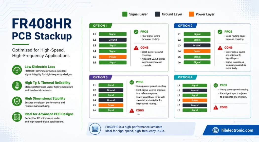
Assign Layer Functions and Reference Planes
Keep critical signals adjacent to continuous reference planes
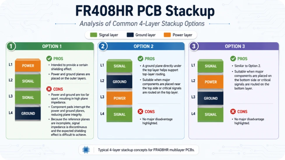
High-speed signals should have a clear return path. Plane splits, voids, reference changes, connector cutouts, and dense via fields can increase return-path inductance and mode conversion even when the trace impedance is nominally correct.
Use symmetry to support dimensional and mechanical stability
A symmetrical layer arrangement does not guarantee a flat board, but it provides a stronger starting point. Copper weight, copper coverage, dielectric thickness, plane distribution, and component-side assembly imbalance should all be considered.
Separate signal-integrity and power-integrity objectives
Closely spaced power-ground pairs can increase plane capacitance, while thick signal-to-plane dielectrics can reduce trace capacitance and alter routing geometry. A stackup should allocate layer pairs deliberately rather than repeating a generic signal-plane pattern.
Plan reference transitions before routing
A signal that changes reference plane needs a nearby return-current path, usually through ground stitching or an appropriate power-to-ground decoupling path. The stackup determines whether that path can be implemented near the signal via.
FR408HR Core, Prepreg and Pressed-Thickness Selection
Available core and prepreg constructions must be reconciled with copper distribution, resin demand, finished thickness and impedance. Nominal catalog thickness is not automatically the dielectric thickness used in the finished-board field solver.
Select Buildable Core and Prepreg Constructions
Core thickness is relatively defined; prepreg thickness is predicted
A copper-clad core arrives as a cured dielectric with a nominal thickness and copper foil. A prepreg becomes the bonding dielectric during lamination. The stackup model should distinguish those two sources of thickness uncertainty.
The broader prepreg material for multilayer PCB guide explains glass style, resin content and bonding behavior, while PCB laminate construction provides the general core-versus-prepreg framework.
Glass style and resin content affect Dk and local behavior
Higher resin content usually lowers the composite Dk because resin and glass contribute differently. It can also change flow and thickness behavior. The design should not choose a construction solely for a lower Dk without considering resin demand, dimensional stability, availability, and processing margin.
Multiple prepreg plies are not electrically identical to one thick ply
Two or more plies can improve resin volume or create a target thickness, but they also change glass distribution and may create resin-rich interfaces. The final field-solver model should use the composite dielectric behavior agreed with the fabricator.
Availability can determine the practical stackup
A theoretically ideal construction may require special procurement or poor sheet utilization. Early engagement with the manufacturer can identify standard stocked cores and prepregs that meet the electrical objective with lower schedule risk.
Model Pressed Thickness and Resin Demand
Pressed thickness is one of the most common differences between a design stackup and a production stackup. It is affected by the prepreg’s resin content, glass style, the copper height on both adjacent layers, the percentage and distribution of copper, press flow, and cure.
Copper coverage percentage is not enough
Two layers can have the same total copper percentage but very different local topography. A broad empty region next to a solid plane creates a different resin-flow problem from uniformly distributed traces. Manufacturers may use local copper maps or experience from similar patterns rather than a single average percentage.
Heavy copper consumes more resin and changes geometry
Thick inner-layer copper creates deeper valleys. The prepreg must fill those valleys without leaving voids or glass stop. More resin or additional prepreg plies may be required, which changes the dielectric thickness and impedance.
Finished thickness tolerance should be realistic
The total board thickness includes cores, pressed prepregs, copper, plating, solder mask, and process variation. A very tight total-thickness requirement can conflict with impedance or resin-flow margin. Identify whether the tolerance is mechanically necessary or merely inherited from a generic drawing template.
Factors Affecting Finished Impedance and Insertion Loss
Finished impedance is the result of the complete geometry and material system. Trace width, etched profile, copper thickness, plating, solder mask, dielectric height, effective Dk, glass weave, copper roughness, reference-plane continuity and via transitions all contribute.
Field-Solver Inputs for Controlled Impedance
| Input | Why it matters | Typical source |
|---|---|---|
| Trace width and spacing | Sets single-ended impedance and differential coupling. | Design constraint plus fabricator compensation. |
| Finished copper thickness | Changes conductor cross-section, spacing at the trace sidewall, and loss. | Copper specification and plating model. |
| Dielectric height | Strongly influences impedance and coupling. | Fabricator’s core/prepreg and pressed-thickness model. |
| Construction-specific Dk | Determines electric-field energy and phase velocity. | Isola table, design characterization, or factory model. |
| Solder mask | Lowers outer-layer impedance and changes loss. | Mask supplier data and factory cured-thickness model. |
| Copper roughness | Increases conductor loss and can affect effective delay. | Foil type, supplier data, or characterized roughness model. |
| Etch profile | Real traces are trapezoidal rather than perfect rectangles. | Factory process model and microsection history. |
Do not mix incompatible Dk methods without documenting the change
Clamped stripline, Bereskin stripline, resonator, differential phase length, and other methods can produce different values because they measure different structures and include different effects. The field solver and acceptance model should use values appropriate to the intended purpose.
Impedance tolerance should reflect total process capability
Trace width, dielectric height, copper thickness, and Dk all vary. A tight impedance tolerance may require wider process margin, more restrictive material construction, tuned artwork, dedicated coupons, or tighter production controls. The tolerance should be driven by system need, not copied automatically from another project.
Differential Pairs, Glass Weave and Intra-Pair Skew
Differential impedance is not the only differential-pair concern. If one conductor sees a different local glass/resin environment than the other, propagation delay can differ and create intra-pair skew. Spread-weave materials reduce local contrast but do not make the PCB isotropic at every trace position.
Mitigation options
- Route critical pairs at a small angle to the primary glass direction where layout permits.
- Use wider traces that average a larger material area.
- Select spread-weave constructions with appropriate resin distribution.
- Keep pair geometry and reference environment consistent.
- Use skew budgeting and channel simulation rather than relying on a single rule.
These options can conflict with routing density, length matching, panel utilization, and fabrication. Apply them to channels that need them rather than to every differential pair.
Where FR408HR Fits in the Channel-Loss Budget
FR408HR is positioned as a mid-loss material. It can support many high-speed digital designs, but no material name defines a universal data-rate limit. The acceptable channel depends on length, frequency content, connectors, vias, copper profile, trace geometry, temperature, equalization, and the transmitter/receiver budget.
Separate dielectric loss from conductor loss
Df influences dielectric loss. Copper roughness, trace dimensions, and current crowding influence conductor loss. As frequency rises, roughness can become a major contributor. A design that selects FR408HR for improved Df but ignores foil profile can miss the expected benefit.
Backdrilling can matter more than a small Df difference
Long via stubs create resonances and loss. For some channels, removing the stub or redesigning the layer transition produces more benefit than changing laminate. Stackup, via architecture, and material should be optimized together.
Know when to move to a lower-loss material
If the channel model has insufficient margin after realistic connector, via, roughness, and manufacturing variation are included, evaluate a lower-loss Isola material or a hybrid construction. The decision should be based on measured or modeled channel performance, not on the label “high speed.”
Example FR408HR Stackup Architectures
The following examples are functional layer arrangements for engineering discussion, not released production stackups. Final dielectric thicknesses, glass styles, copper weights and trace geometries must be modeled against the actual board requirements and material availability.
The examples below show layer-function logic, not released production stackups. They deliberately omit fixed dielectric thicknesses and trace widths because those values must be solved from the target impedance, finished copper, selected FR408HR construction, panel process and available material.
Six-layer control and interface board
| Layer | Primary function | Engineering intent |
|---|---|---|
| L1 | Components and controlled surface signals | Reference critical routes to the continuous L2 ground plane. |
| L2 | Ground plane | Provide a low-inductance return path and shielding for L1/L3. |
| L3 | Internal signals | Route controlled stripline or mixed signal according to spacing and reference needs. |
| L4 | Power plane / low-speed routing | Keep plane splits away from critical return paths. |
| L5 | Ground plane | Reference L6 and support structural symmetry with L2. |
| L6 | Components and secondary signals | Balance outer copper and reserve short controlled routes where needed. |
Review focus: outer-layer copper balance, L3/L4 coupling, plane splits, through-via stubs and whether the six-layer architecture provides enough continuous references for every critical route. A general 6-layer PCB stackup reference can help compare plane and routing roles, but the FR408HR construction still requires its own impedance model.
Eight-layer high-speed digital board
| Layer pair | Suggested role | Why it is used |
|---|---|---|
| L1 / L2 | Surface high-speed signals over ground | Provides a direct microstrip reference and controlled return path. |
| L3 / L4 | Internal signal over plane | Supports stripline routing and isolates critical channels from the outer surface. |
| L5 / L6 | Power distribution and internal signals | Balances the upper half and creates an additional referenced routing layer. |
| L7 / L8 | Ground and bottom signals/components | Provides a controlled bottom microstrip environment and mechanical symmetry. |
Review focus: whether each signal layer has one dominant continuous reference, how transitions stitch return current, whether power-plane placement supports the PDN, and whether outer and inner controlled geometries can share the requested tolerance. Compare the functional arrangement with Highleap’s 8-layer PCB stacking guide before freezing layer assignments.
Twelve-layer processing, networking or backplane board
A twelve-layer FR408HR board normally needs a more explicit signal-class allocation rather than a simple alternating signal/plane pattern. One workable functional approach is: For a related high-layer-count reference, see the 10-layer PCB stackup discussion and adapt the principles rather than copying dimensions.
L1   Components / short high-speed routes
L2   Ground
L3   High-speed stripline group A
L4   Ground or power reference
L5   Medium-speed / control routing
L6   Power
L7   Ground
L8   Medium-speed / control routing
L9   Ground or power reference
L10  High-speed stripline group B
L11  Ground
L12  Components / short high-speed routes
Review focus: layer-pair symmetry, connector breakouts, high-speed layer grouping, plane transition strategy, power integrity, glass-weave exposure, through-via stubs, backdrill depth, sequential-lamination need, resin demand and registration accumulation. If the board requires multiple lamination cycles or blind/buried vias, the architecture must be reviewed together with the planned multilayer fabrication route.
FR408HR Impedance Coupon and TDR Testing
A production coupon should represent the manufactured transmission line closely enough to provide actionable feedback. Coupon location, copper build, dielectric construction, reference plane, test method and acceptance tolerance should be agreed before panelization.
The coupon must represent the board construction
Coupon layers, reference planes, dielectric construction, copper plating, solder mask, trace orientation, and processing should correspond to the production structure. A coupon placed in an unrepresentative panel region can pass while the product region behaves differently.
The measurement window must exclude launch artifacts
Connector or probe launch, coupon transitions, and end reflections can distort the result. Coupon design and test setup should provide a stable section long enough for evaluation.
Agree on reporting before production
The report should identify target, tolerance, measured value, layer or structure, coupon ID, lot, date, and method. If raw traces, plots, or calibration evidence are required, include them in the quotation.
TDR validates impedance, not insertion loss
A passing impedance coupon does not prove that the complete routed channel meets loss or eye-diagram requirements. Use appropriate test vehicles, VNA methods, or system validation when the product needs channel-loss evidence.
Stackup Review, Common Errors and Fabrication Handoff
The final design review should close the gap between the EDA stackup and the fabricator’s build record. Common errors include using an inappropriate Dk, assuming unavailable prepreg thicknesses, modeling base copper instead of finished copper, omitting solder mask, breaking reference planes and freezing the layout before the production construction is approved.
Review Checklist Before Layout Freeze
- Confirm that FR408HR is required and that substitution rules are explicit.
- Identify all controlled-impedance structures by layer and reference plane.
- Define target, tolerance, nominal geometry, and allowed manufacturing adjustment.
- Ask the fabricator to select real core and prepreg constructions.
- Use construction-appropriate Dk/Df and document the method.
- Review finished copper, foil profile, solder mask, and etch geometry.
- Check layer symmetry, copper balance, power-plane assignment, and return paths.
- Review via spans, aspect ratios, backdrill, and reference transitions.
- Model insertion loss with realistic connector, via, and copper assumptions.
- Approve the production stackup and coupon before routing is frozen or tooling begins.
Controlled Handoff to Fabrication
The stackup page ends where chronological process control begins. After the design team approves layer functions, target impedance and candidate core/prepreg constructions, the fabricator must confirm material availability, pressed-thickness assumptions, artwork compensation, panel coupons and the actual lamination route.
| Stackup output | Required manufacturing confirmation | Release evidence |
|---|---|---|
| Selected core and prepreg | Availability, glass style, resin content, ply count and pressed-thickness model. | Approved production stackup. |
| Controlled impedance geometry | Finished copper, etch compensation, solder mask and allowed trace tuning. | Impedance table and CAM approval. |
| Via and reference transitions | Drill sizes, plating allowance, backdrill depth, registration and return-path stitching. | Fabrication drawing and controlled-depth notes. |
| TDR coupon strategy | Coupon location, representative construction, launch, test window and reporting. | Coupon drawing and acceptance criteria. |
After stackup approval, confirm lamination, drilling, plating, inspection, and via-structure requirements in the fabrication package before release.
FR408HR Stackup FAQ, References and Engineering Review
This section addresses recurring design questions, identifies the role of relevant standards and test references, and explains what information should be sent for stackup review.
Frequently Asked Questions
What Dk should be used for FR408HR?
Use a value tied to the selected core or prepreg construction, frequency range, and modeling method. The commonly cited general value is not appropriate for every construction. The manufacturer and design team should document the production value used for impedance calculation.
Can the same Dk be used for core and prepreg?
Not automatically. Core and prepreg constructions can have different glass styles and resin contents. Prepreg also has pressed-thickness uncertainty. Use construction-specific data and the fabricator’s model.
Does FR408HR require a special impedance-coupon method?
No unique method is required solely because of the material, but the coupon must represent the actual construction and finished copper. Reporting and acceptance should be agreed before production.
Is FR408HR suitable for PCIe, Ethernet, DDR, or SerDes?
It can be suitable for many implementations, but the interface name alone is not enough. Data rate, channel length, topology, connectors, vias, loss budget, equalization, and manufacturing variation determine suitability.
Should a stackup page include quotation content?
Stackup, Modeling and Test References
The sources below support the material and standards discussion on this page. Supplier data-sheet values are typical values measured under stated methods; the customer drawing, purchase order, approved stackup, and contractually specified standard revision remain the controlling requirements for production acceptance.
- Isola FR408HR Dk/Df construction tables — Core and prepreg values by construction, resin content, thickness and frequency.
- Isola FR408HR data sheet — General frequency-dependent Dk/Df values and test methods.
- IPC-2141 — Controlled-impedance and high-speed design guidance; use field-solver modeling and production feedback for final geometry.
- IPC-2221 / IPC-2222 — Generic and rigid-board design requirements that frame stackup, conductor, spacing, hole and documentation decisions.
- IPC-TM-650 — Test-method library for material and printed-board measurements; the exact method must be stated when results are compared.
Submit a Stackup for Engineering Review
Send the layer functions, finished thickness, starting and finished copper, controlled-impedance table, nominal trace geometry, critical channel information, via architecture and production quantity. Highleap can map the conceptual construction to available FR408HR cores and prepregs and identify the dimensions that require written approval before layout freeze or tooling.
Connect the approved FR408HR stackup to a manufacturing quotation.

Recommended Posts

Taconic RF 35 vs RO4350B PCB
Table of contentsRF-35 vs RO4350B Procurement and...

TMM4 Filter PCB Manufacturing
TMM4 filter PCB manufacturing is controlled by the...

TMM3 PCB Manufacturing for RF Modules
TMM3 PCB manufacturing is most useful where the RF module...

TMM6 PCB Fabrication
TMM6 fabrication is the process-control page for a mid-Dk...
How to get a quote for PCBs
Let’s run DFM/DFA analysis for you and get back to you with a report. You can upload your files securely through our website. We require the following information in order to give you a quote:
-
- Gerber, ODB++, or .pcb, spec.
- BOM list if you require assembly
- Quantity
- Turn time
For PCBA services, please provide your BOM (Bill of Materials) and any specific assembly instructions. We also offer DFM/DFA analysis to optimize your designs for manufacturability and assembly, ensuring a smooth production process.