
Taconic RF-60A PCB Manufacturer for Compact High-Dk RF
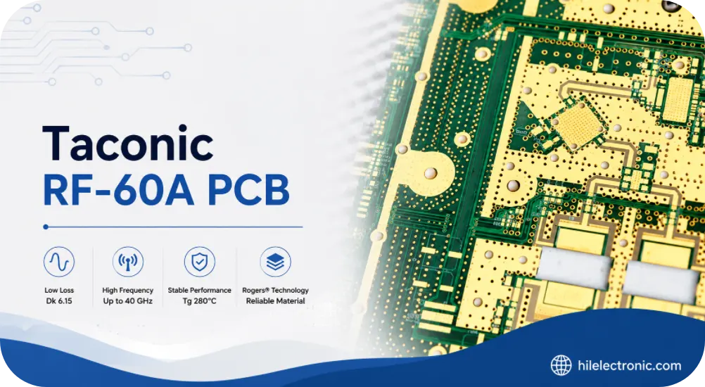
Highleap Electronics manufactures Taconic RF-60A PCB solutions for compact antennas, filters, couplers, resonators, matching networks, satellite circuits and high-power RF modules. Production support includes high-Dk geometry review, tight coupled-gap control, plated RF grounds, precision mechanical interfaces, connector assembly and customer-defined testing.
Because RF-60A is a legacy designation, Highleap confirms the controlled material, available thickness, copper, certificates and approved transition rules before quotation. Current AGC RF-60TC is a separate Dk-6.15 thermally conductive laminate; it can be evaluated as an alternative only through documented customer approval.
RF-60A and Current RF-60TC Characteristics for Compact RF
Dk-6-class materials allow smaller resonators, antennas and matching structures, but they also make dimensional variation more electrically significant. Current AGC RF-60TC is a PTFE-based, ceramic-filled fiberglass substrate with Dk 6.15 ± 0.15, Df 0.002 and thermal conductivity 1.05 W/m·K. Those published values apply to RF-60TC, not automatically to a legacy RF-60A drawing.
| Characteristic | Product impact | Highleap manufacturing response |
|---|---|---|
| High dielectric constant | Enables compact RF structures and shorter electrical length. | Flag critical gaps, resonator dimensions and registration as controlled characteristics. |
| Low dielectric loss | Supports filters, dividers, amplifiers and antenna structures at microwave frequencies. | Review copper profile, finish and conductor geometry with the material loss model. |
| Thermal conductivity in RF-60TC | Supports heat spreading in power RF and compact layouts. | Review copper/ground interface, component thermal path and assembly process. |
| Legacy-to-current transition risk | A similar Dk class does not prove identical tuning or qualification. | Require customer approval of stackup, artwork impact, RF verification and documentation. |
Reference the official AGC RF-60TC product data and Highleap’s high-Dk PCB material guidance when reviewing a current production route.
Taconic RF-60A PCB Manufacturing Capabilities
Highleap manufactures customer-controlled RF-60A circuits for compact antennas, couplers, filters, resonators, matching networks, wearable/medical RF devices and other designs that use a high dielectric constant to reduce physical wavelength and circuit size. We support two-layer, plated-through-hole, multilayer hybrid, edge-plated and assembled RF modules subject to DFM.
Highleap Support for Compact Dk-6-Class RF Circuits
| Project area | Highleap project support |
|---|---|
| Circuit types | Compact patch antennas, filters, couplers, dividers, resonators and power-amplifier boards |
| Critical dimensions | Tight line/gap, coupled structures, resonator features and RF launch geometries |
| Grounding/PTH | Dense via fences, thermal grounds, connector grounds and representative microsection inspection |
| Mechanical features | Precision routing, connector locations, mounting holes, cavities and metal-interface requirements |
| PCBA | Power RF devices, MMIC/QFN, passives, connectors, shields and thermal hardware |
| Quality/test | Dimensional reports, electrical test, agreed impedance/RF evidence and customer-defined test |
Highleap Rigid RF PCB Manufacturing Capabilities
The figures below are Highleap’s published rigid-PCB factory limits. High-Dk RF-60A structures often use narrow coupled gaps and compact resonators, so final manufacturability is confirmed from the exact material, copper, etch tolerance and inspection plan. See the complete Highleap rigid PCB capability table for the published factory specification.
| Manufacturing item | Published Highleap capability | RF/PTFE project condition |
|---|---|---|
| Maximum layer count | Up to 60 layers | Layer count for a specific RF/PTFE or hybrid stackup is confirmed after lamination, registration, via and material review. |
| Minimum inner-layer trace/space | 2/2 mil (0.05/0.05 mm) | The released RF geometry also depends on copper thickness, foil type, etch compensation and critical-dimension tolerance. |
| Minimum outer-layer trace/space | 2/2 mil (0.05/0.05 mm) | Fine RF gaps and coupled structures require project-specific feasibility and inspection criteria. |
| Board thickness range | 0.2–8.0 mm | Available thickness for a named Taconic/AGC construction depends on laminate gauge, bonding method and approved stackup. |
| Board-thickness tolerance | ±0.1 mm below 1.0 mm; ±10% at 1.0 mm and above | RF connector launches and enclosure interfaces should state any tighter product-level requirement. |
| Minimum finished board size | 10 × 10 mm | Small circuits may require delivery in a manufacturing panel or array for fabrication and assembly. |
| Maximum finished board size | 22.5 × 47.5 in (571.5 × 1206.5 mm) | Large-format PTFE boards require separate review for material sheet size, registration, flatness, routing and shipment. |
| Minimum mechanical drill / annular ring | 0.15 mm / 0.127 mm | Final via design depends on board thickness, aspect ratio, plating requirement and material-specific drilling process. |
| Minimum laser drill / annular ring | 0.075 mm / 0.075 mm | Laser microvias are subject to dielectric thickness, capture-pad design, copper build and sequential-lamination review. |
| Mechanical-drill aspect ratio | Up to 20:1 | The achievable ratio for an RF/PTFE build must be confirmed with finished hole size, board thickness and plating requirement. |
| Laser-drill aspect ratio | 1:1 | Microvia geometry is released only after stackup and reliability review. |
| Maximum inner/outer copper | Up to 10 oz | Maximum copper cannot automatically be combined with the finest trace/space or every PTFE construction. |
| PTH / NPTH tolerance | PTH ±0.075 mm; NPTH ±0.05 mm | Connector and RF grounding holes should identify finished diameter and any tighter fit requirement. |
| Contour tolerance | ±0.1 mm | Edge launches, cavities, slots and connector locations may need a dedicated dimensional-control plan. |
| Controlled-impedance tolerance | Single-ended and differential: ±5 Ω at ≤50 Ω; ±7% above 50 Ω | The quoted tolerance applies to an approved stackup, coupon strategy and measurement method. |
| Available surface finishes | ENIG, ENEPIG, OSP, HASL, immersion silver, immersion tin, flash gold, hard gold and gold fingers | Finish selection is reviewed for RF loss, soldering, wire bonding, connector contact and environmental requirements. |
Capability-combination notice: values in the table are individual factory capability limits. Layer count, 2/2 mil geometry, 10 oz copper, maximum panel size, 20:1 aspect ratio and the thinnest board construction are not assumed to be simultaneously achievable. Highleap confirms the usable combination after reviewing the exact material, stackup, copper, drill, RF tolerance, surface finish and assembly package.
RF-60A is a legacy Taconic designation that continues to appear in the AGC technical library. The current AGC main RF table lists RF-60TC rather than RF-60A. Highleap verifies the exact drawing requirement, stock, certificates and approved substitution policy using the current AGC RF/microwave portfolio. RF-60TC or another Dk-6-class material is not used as an automatic replacement.
Production is coordinated through Highleap’s microwave PCB manufacturing service with a route specific to the supplied laminate and geometry.
Why High-Dk Circuits Need Tighter Dimensional Discipline
A high-Dk laminate enables smaller resonators and antennas, but the compact geometry can make frequency response more sensitive to etch variation, dielectric thickness, copper, plating and surface finish. Highleap identifies resonant lengths, coupled gaps, feed points and ground structures as critical features during CAM review.
| High-Dk design feature | Production sensitivity | Highleap control |
|---|---|---|
| Short resonator length | Small dimensional change can shift frequency | Critical-dimension compensation and first-article measurement. |
| Narrow coupled gap | Etch bias changes coupling and bandwidth | Controlled artwork compensation and gap inspection. |
| Compact antenna feed | Registration affects match and radiation | Datum-based drilling/routing and launch inspection. |
| Dense ground vias | Hole position and copper affect return path | Drill registration, hole copper and electrical verification. |
| Thin dielectric | Handling and thickness tolerance affect impedance | Material incoming check, process support and stackup control. |
| Plated edge or cavity | Mechanical/plating tolerance affects enclosure interface | Dedicated drawing dimensions and inspection plan. |
The design and fabrication trade-offs are further explained in RF PCB miniaturisation techniques and RF PCB tolerance control.
Material and Impedance Release Before Tooling
The RFQ must state whether the customer’s impedance and RF model use nominal, process or design Dk, and at what frequency or method. Highleap will not assume that a legacy RF-60A data value can be replaced by a current RF-60TC value. The controlled stackup and material document govern production.
RF-60A Material Availability and RF-60TC Approval
Highleap keeps the original RF-60A route and any RF-60TC proposal separate. The proposed transition records electrical model, thickness, copper, thermal behaviour, PTH process, artwork impact, qualification and certificate requirements. Only the customer-authorised route is released to purchasing and production.
- confirm exact grade, manufacturer identity, thickness, tolerance, copper and lot documentation;
- identify critical RF lines, resonators, coupling gaps and phase-sensitive structures;
- include finished copper and solder-mask condition in the geometry model;
- define impedance structures and reports using RF impedance control;
- define material substitution and design-change authority in writing;
- record the approved construction for repeat-order traceability.
When the material is under evaluation, Highleap can compare manufacturable options through the RF PCB material comparison. Final selection and qualification remain with the design owner.
Fabrication and Quality Controls for Compact RF Structures
Highleap assigns process controls according to the actual frequency, geometry and acceptance criteria. A compact Dk-6 circuit may require more dimensional evidence than a physically larger low-Dk board even when both use simple two-layer construction.
- line and gap measurement on selected resonators, couplers and matching structures;
- dielectric-thickness and finished-board-thickness verification;
- controlled drill registration for ground vias and connector references;
- plated-through-hole microsection when hole reliability is a project risk;
- impedance coupon or customer-defined test vehicle;
- surface-finish selection using RF and microwave surface-finish guidance;
- electrical test plus optional RF verification as described in RF PCB testing.
Quality evidence is agreed before quotation. Highleap can provide material traceability, electrical test, selected dimensional results, microsections, impedance records, first-article inspection and customer-specified RF test results when included in the order.
RF-60A PCB Assembly and Thermal/Mechanical Integration
Highleap can assemble RF-60A boards with RF passives, amplifiers, mixers, oscillators, connectors, shields, heat spreaders and mechanical hardware. High-Dk miniaturisation often places components and grounding features close together, so stencil, solder volume, rework access and connector alignment must be reviewed early.
| Assembly area | Control |
|---|---|
| Exposed-pad RF ICs | Paste aperture, via treatment, reflow and X-ray acceptance. |
| Power devices | Thermal interface, copper/ground path, reflow profile and heat-sink attachment. |
| RF connectors | Edge geometry, board thickness, alignment, soldering and mechanical fit. |
| Shields and cavities | Coplanarity, grounding, solder process and final enclosure fit. |
| Fine matching components | Placement accuracy, orientation, controlled rework and revision traceability. |
| Functional/RF test | Defined fixture, calibration, serialisation and acceptance limits. |
Power-amplifier projects can be reviewed with Highleap’s power-amplifier PCB manufacturing and RF assembly process controls.
RF-60A Lead Time, Material Continuity, and Quotation
Lead time is issued after Highleap confirms legacy RF-60A material, customer-supplied stock or an approved transition route. The quotation identifies engineering release, material-ready, bare-board, first-assembly and final-shipment milestones. Split delivery can be used when early RF validation is required.
For a complete PCB and PCBA route, Highleap can combine the RF laminate review with RF PCB assembly engineering and a formal production quotation.
Quotation and lead time are confirmed after material status, critical-dimension feasibility, assembly thermal requirements and test readiness are closed. Where an alternative requires tuning or RF validation, Highleap quotes the qualification build separately from recurring production.
Send Gerber/ODB++, fabrication drawing, controlled material specification, stackup, critical RF dimensions, impedance or S-parameter requirements, drill/route files, finish, quantities, target delivery, BOM, assembly drawings and test method through Highleap Electronics. For urgent builds, request evaluation through fast high-frequency PCB manufacturing.
Can Highleap manufacture legacy Taconic RF-60A?
Yes, after approved material availability, thickness, copper, documents and substitution rules are confirmed.
Can RF-60TC replace RF-60A?
Not without approval. The current material has its own Dk tolerance, loss, thermal properties, thicknesses and qualification status.
Can Highleap hold tight coupled gaps?
Highleap reviews the actual copper, geometry, panel layout and acceptance method, then returns manufacturable tolerances and any required first-article measurement.
Can RF-60A PCB and assembly be quoted together?
Yes. Component sourcing, assembly, inspection, mechanical integration and customer-defined testing can be included.
What data is needed for an RF-60A PCB quotation?
Provide the controlled material specification, Gerber/ODB++, stackup, copper, critical geometry table, frequency range, impedance or tuning requirements, thermal interface, quantities, assembly files and test limits.
Can Highleap support compact high-Dk RF PCB assembly?
Yes. Highleap can quote component sourcing, controlled paste and reflow, RF connector and shield installation, inspection, cleaning, thermal hardware and customer-defined functional or RF testing.

Recommended Posts

Isola Astra MT77 PCB Manufacturing
Figure 1. Isola Astra MT77 PCB ManufacturingIsola Astra...

Nelco N4000-13 PCB Material and Manufacturing Guide | Highleap Electronics
Figure 1. Nelco N4000-13 PCBNelco N4000-13 PCB is a...

Copper Clad Laminate: Complete Material Selection Guide for PCB Engineers
Every electrical property that matters in a printed...

Inside a China Ceramic PCB Factory: Process Control Across Power/LED/RF/Medical
Table of Contents Inside a China Ceramic PCB Factory: How...
How to get a quote for PCBs
Let’s run DFM/DFA analysis for you and get back to you with a report. You can upload your files securely through our website. We require the following information in order to give you a quote:
-
- Gerber, ODB++, or .pcb, spec.
- BOM list if you require assembly
- Quantity
- Turn time
For PCBA services, please provide your BOM (Bill of Materials) and any specific assembly instructions. We also offer DFM/DFA analysis to optimize your designs for manufacturability and assembly, ensuring a smooth production process.