
Power Amplifier PCB Design for Audio and RF Applications

Power amplifier PCBs demand different design approaches depending on whether you’re amplifying audio or RF signals. While both deal with power delivery and thermal management, the similarity ends there. After manufacturing amplifier PCBs from 1W Bluetooth speakers to 5kW broadcast transmitters, here’s what makes the difference between clean amplification and distorted disappointment.
How to Layout Class D Amplifier PCB for Low THD
Class D amplifiers dominate modern audio due to superior efficiency, but PCB layout determines whether you get HiFi sound or AM radio interference. The switching stage generates square waves with harmonics extending into MHz ranges—proper layout contains these signals while preserving audio quality.
Critical Class D power amplifier PCB layout rules:
- Output filter inductors must be shielded types positioned away from input stages
- Bootstrap capacitors locate within 5mm of high-side drivers
- Differential inputs route as matched impedance pairs
- Power and ground planes provide return paths for switching currents
A recent automotive audio amplifier achieved 0.01% THD by optimizing ground current paths. The same circuit with poor layout showed 0.5% THD and failed EMI testing spectacularly. These layout principles also apply to switch mode power supply PCB designs using similar switching topologies.
50 Ohm Impedance Matching for RF Power Amplifier PCB
RF power amplifiers convert most input power into heat, making thermal design critical. But unlike audio amplifiers, RF circuits require precise impedance matching throughout signal paths. A few picofarads of stray capacitance can destroy matching networks carefully designed for 50Ω systems.
For cellular base station designs:
- Use Rogers or PTFE materials for consistent dielectric properties
- Implement coplanar waveguides for controlled impedance
- Place thermal vias directly under LDMOS or GaN devices
- Add quarter-wave stubs for harmonic termination
We manufacture with specialized PCB laminate materials for RF applications, maintaining dielectric constant tolerance within ±2% for predictable performance. These materials are also crucial for high efficiency power PCB designs operating at high frequencies.
How to Eliminate Ground Loop Hum in Audio Amplifier PCB
High-end audio amplifiers still use linear designs for ultimate sound quality. These circuits are particularly sensitive to grounding issues that cause hum, oscillation, or poor channel separation. Star grounding works but requires careful implementation to avoid ground loops.
Effective grounding for audio applications:
- Separate ground paths for power, signal, and speaker returns
- Connect grounds at single point near power supply
- Use ground planes for shielding, not current carrying
- Implement balanced inputs for professional audio applications
These grounding strategies also benefit power electronics PCB designs where noise isolation is critical.
Capacitor Placement Guidelines for Power Amplifier PCB
Amplifiers require clean, stiff power supplies for optimal performance. But traditional bulk capacitors aren’t enough—proper decoupling requires multiple capacitor values positioned strategically across the PCB.
Decoupling hierarchy for power amplifier designs:
- 10,000µF+ bulk storage at power input
- 100-470µF low-ESR capacitors at each amplifier stage
- 0.1µF ceramics within 10mm of active devices
- 1000pF COG/NPO capacitors for RF bypassing
For switching amplifiers, add dedicated filter sections with common-mode chokes to prevent conducted emissions from contaminating power lines. This approach mirrors techniques used in AC-DC converter PCB input filtering.

Speaker Protection Circuit Design for Audio Amplifier PCB
Amplifier protection must respond quickly enough to save expensive output devices without false triggering during normal operation. Simple current limiting isn’t sufficient—modern protection monitors multiple parameters simultaneously.
Essential protection features:
- SOA (Safe Operating Area) protection for output transistors
- DC offset detection prevents speaker damage
- Thermal shutdown with hysteresis
- Output crowbar for catastrophic failures
We’ve seen too many amplifier failures from inadequate protection. Proper PCB assembly includes testing protection circuits at extremes—not just verifying they exist. These protection philosophies extend to power regulation PCB designs as well.
How to Mount Heatsink on Power Amplifier PCB
Power amplifiers generate heat proportional to output power and inefficiency. Class AB amplifiers might dissipate 60% of input power as heat. Even efficient Class D designs need thermal management for reliability.
Thermal design guidelines:
- Calculate worst-case dissipation at maximum power and temperature
- Use thermal modeling to verify junction temperatures
- Apply thermal compound consistently—voids create hot spots
- Consider forced air cooling above 100W continuous power
For broadcast transmitter applications, we use insulated metal substrates (IMS) providing direct heat path to chassis-mounted heatsinks. Similar thermal solutions benefit power inverter PCB designs with high power density.
Reducing EMI in Class D Amplifier PCB Design
Power amplifiers are EMI generators by nature—they’re designed to efficiently deliver power at specific frequencies. Containing emissions without affecting performance requires targeted filtering and shielding.
For switching amplifier designs, input filtering prevents switching noise from modulating audio signals. Shield sensitive input stages from power supply magnetic fields. Use twisted pairs for signal routing where differential signaling isn’t possible.
Trust Highleap Electronics for electronic manufacturing service that understands amplifier requirements. From prototypes to production, we ensure your power amplifier PCBs deliver specified performance reliably.
FAQ
Q1: What materials are best for Power Amplifier PCB manufacturing?
A: For audio amplifiers, FR-4 is often sufficient, but for high-frequency RF power amplifiers, low-loss materials such as Rogers, PTFE, or ceramic-filled laminates are preferred. These materials provide stable dielectric properties, minimize insertion loss, and maintain consistent impedance at GHz frequencies.
Q2: How many PCB layers are recommended for a Power Amplifier PCB?
A: Most low- to mid-power audio amplifier PCBs work well with 2-layer designs. High-power or RF amplifiers benefit from 4-layer or 6-layer stack-ups, allowing for solid ground planes, controlled impedance traces, and reduced parasitic inductance for stable high-frequency operation.
Q3: What is the typical copper thickness used in Power Amplifier PCBs?
A: 1oz copper is standard for small audio amplifier PCBs, but high-power designs often require 2oz or even 3oz copper to handle high currents without excessive temperature rise. Thicker copper also improves thermal conductivity, which is critical for reliability.
Q4: Can Power Amplifier PCBs be manufactured with aluminum base for better heat dissipation?
A: Yes. Metal Core PCBs (MCPCBs) or IMS (Insulated Metal Substrate) boards are commonly used for high-power RF and Class D amplifiers to provide direct thermal paths to heatsinks. This reduces junction temperature and allows more compact designs.
Q5: What surface finish is recommended for Power Amplifier PCBs?
A: ENIG (Electroless Nickel Immersion Gold) is preferred for power amplifier PCBs due to its flat surface and excellent corrosion resistance. For RF applications, ENEPIG can offer even better wire-bonding performance, while HASL may be acceptable for cost-sensitive audio applications.
Q6: How to ensure signal integrity when manufacturing Power Amplifier PCBs?
A: Work with a PCB manufacturer that supports impedance control, tight layer-to-layer registration, and precise trace width tolerances. Consistent manufacturing quality ensures that designed impedance networks work as simulated, avoiding unwanted distortion or mismatch losses.

Related Articles

Underwater & Pool LED Light PCBs: IP68 Potted Boards, Low-Voltage Drivers & Safety
Figure 1. LED pool light PCB manufacturing reference....
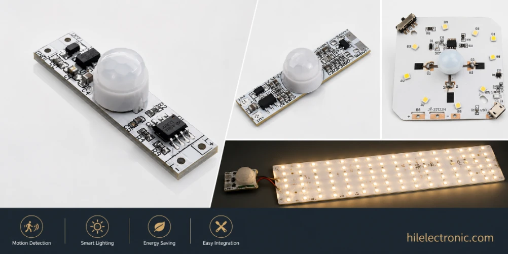
Motion Sensor & Smart LED Light PCBs: Sensor, Control, Driver & Wireless Boards
Figure 1. motion sensor LED light PCB manufacturing...

LED High Bay Light PCBs: Metal-Core Light Engines, Drivers & Turnkey Boards Built to Spec
Figure 1. LED high bay light PCB manufacturing reference....
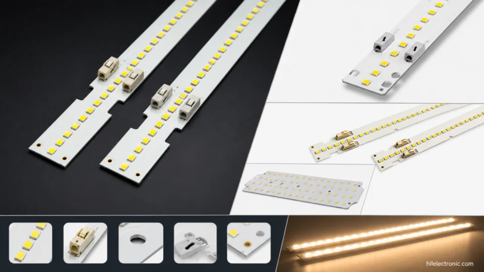
LED Linear & Strip Light PCBs: Long-Format Engines, Flexible & Rigid-Flex Boards
Figure 1. LED linear light PCB manufacturing reference....
How to get a quote for PCBs
Let us run DFM/DFA analysis for you and get back to you with a report.
You can upload your files securely through our website.
We require the following information in order to give you a quote:
-
- Gerber, ODB++, or .pcb, spec.
- BOM list if you require assembly
- Quantity
- Turn time
In addition to PCB manufacturing, we offer a comprehensive range of electronic services, including PCB design, PCBA (Printed Circuit Board Assembly), and turnkey solutions. Whether you need help with prototyping, design verification, component sourcing, or mass production, we provide end-to-end support to ensure your project’s success. For PCBA services, please provide your BOM (Bill of Materials) and any specific assembly instructions. We also offer DFM/DFA analysis to optimize your designs for manufacturability and assembly, ensuring a smooth production process.