
Taconic TLX-0 PCB Manufacturing and Legacy Production Support
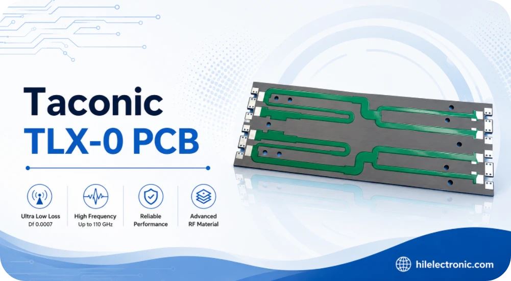
Highleap Electronics manufactures legacy Taconic TLX-0 PCB assemblies for oscillators, MMIC modules, microwave test circuits, RF control boards and service replacements. We support prototype recreation, low-volume continuity, repeat production, controlled file recovery, RF fabrication, connector assembly and customer-defined testing from authorised customer data.
TLX-0 is not treated as a current generic laminate. Before price or delivery is committed, Highleap verifies the original drawing revision, material identification, thickness, copper, available documentation and substitution authority. This protects fielded products from undocumented material or geometry changes.
TLX-0 Legacy Material Characteristics and Drawing Control
TLX-0 appears in older Taconic RF drawings, but current AGC product tables list TLX-8 rather than TLX-0 as the main TLX offering. TLX-8 is a woven-glass PTFE laminate with published Dk 2.55 ± 0.04 and Df 0.0018; it is not automatically the same material or construction as TLX-0.
| Legacy-control item | Why it matters | Highleap action |
|---|---|---|
| Original material identity | An informal TLX label may omit the exact historical grade, thickness or copper. | Use controlled drawings, certificates, purchase records or customer approval to release the material. |
| RF artwork and scale | Old photoplot or Gerber data may include compensation tied to the original process. | Compare data revision, units, aperture information, dimensions and known-good samples. |
| PTH and mechanical construction | Oscillator/MMIC modules may depend on connector, cavity and grounding details. | Release hole, routing, plating and mechanical tolerances before tooling. |
| Substitution authority | A current TLX grade may alter electrical length, tuning or compliance. | Quote the transition as a controlled change with customer-defined verification. |
For current material context, see the official AGC TLX-8 product page. Highleap uses its Gerber file review checklist to close legacy-data gaps before production.
Taconic TLX-0 PCB Manufacturing and Continuity Support
Highleap supports legacy TLX-0 designs used in oscillators, MMIC evaluation circuits, microwave modules and other low-Dk RF products. We can review bare-board reproduction, controlled redesign, small-batch service production, NPI replacement builds and complete assembly. The objective is to preserve the released electrical and mechanical configuration, not reinterpret an old drawing without authority.
Legacy PCB Manufacturing Support at Highleap
| Project area | Highleap project support |
|---|---|
| Data recovery | Review of controlled Gerber, drill, drawings, netlists, stackups and customer-supplied sample records |
| Build-to-print production | Single/double-sided, PTH and customer-approved multilayer/hybrid RF constructions |
| Mechanical replication | Connector locations, routed outlines, cavities, mounting holes and metal-interface features |
| Assembly continuity | BOM review, approved alternates, SMT/THT, RF connectors, shields and programming |
| Verification | First-article dimensions, electrical test, customer-defined functional/RF test and comparison to approved records |
| Repeat-order control | Revision, material, lot and process records retained for subsequent service batches |
Highleap Rigid RF PCB Manufacturing Capabilities
The figures below are Highleap’s published rigid-PCB factory limits. A legacy TLX-0 design is released only after the material identity, thickness, copper, drill data and drawing tolerances are confirmed; an old drawing does not automatically qualify for every listed limit. See the complete Highleap rigid PCB capability table for the published factory specification.
| Manufacturing item | Published Highleap capability | RF/PTFE project condition |
|---|---|---|
| Maximum layer count | Up to 60 layers | Layer count for a specific RF/PTFE or hybrid stackup is confirmed after lamination, registration, via and material review. |
| Minimum inner-layer trace/space | 2/2 mil (0.05/0.05 mm) | The released RF geometry also depends on copper thickness, foil type, etch compensation and critical-dimension tolerance. |
| Minimum outer-layer trace/space | 2/2 mil (0.05/0.05 mm) | Fine RF gaps and coupled structures require project-specific feasibility and inspection criteria. |
| Board thickness range | 0.2–8.0 mm | Available thickness for a named Taconic/AGC construction depends on laminate gauge, bonding method and approved stackup. |
| Board-thickness tolerance | ±0.1 mm below 1.0 mm; ±10% at 1.0 mm and above | RF connector launches and enclosure interfaces should state any tighter product-level requirement. |
| Minimum finished board size | 10 × 10 mm | Small circuits may require delivery in a manufacturing panel or array for fabrication and assembly. |
| Maximum finished board size | 22.5 × 47.5 in (571.5 × 1206.5 mm) | Large-format PTFE boards require separate review for material sheet size, registration, flatness, routing and shipment. |
| Minimum mechanical drill / annular ring | 0.15 mm / 0.127 mm | Final via design depends on board thickness, aspect ratio, plating requirement and material-specific drilling process. |
| Minimum laser drill / annular ring | 0.075 mm / 0.075 mm | Laser microvias are subject to dielectric thickness, capture-pad design, copper build and sequential-lamination review. |
| Mechanical-drill aspect ratio | Up to 20:1 | The achievable ratio for an RF/PTFE build must be confirmed with finished hole size, board thickness and plating requirement. |
| Laser-drill aspect ratio | 1:1 | Microvia geometry is released only after stackup and reliability review. |
| Maximum inner/outer copper | Up to 10 oz | Maximum copper cannot automatically be combined with the finest trace/space or every PTFE construction. |
| PTH / NPTH tolerance | PTH ±0.075 mm; NPTH ±0.05 mm | Connector and RF grounding holes should identify finished diameter and any tighter fit requirement. |
| Contour tolerance | ±0.1 mm | Edge launches, cavities, slots and connector locations may need a dedicated dimensional-control plan. |
| Controlled-impedance tolerance | Single-ended and differential: ±5 Ω at ≤50 Ω; ±7% above 50 Ω | The quoted tolerance applies to an approved stackup, coupon strategy and measurement method. |
| Available surface finishes | ENIG, ENEPIG, OSP, HASL, immersion silver, immersion tin, flash gold, hard gold and gold fingers | Finish selection is reviewed for RF loss, soldering, wire bonding, connector contact and environmental requirements. |
Capability-combination notice: values in the table are individual factory capability limits. Layer count, 2/2 mil geometry, 10 oz copper, maximum panel size, 20:1 aspect ratio and the thinnest board construction are not assumed to be simultaneously achievable. Highleap confirms the usable combination after reviewing the exact material, stackup, copper, drill, RF tolerance, surface finish and assembly package.
AGC’s technical library still references TLX-0 in legacy oscillator work, while the current main RF product table lists TLX-8 as the active TLX product. See the AGC technical-article library and current TLX-8 product page. Highleap verifies whether the order requires original TLX-0 stock, customer-supplied material, or an approved transition. TLX-8 is not assumed to be a drop-in replacement.
The production release follows Highleap’s fabrication-file review checklist so legacy notes, stackup, drill data, material callouts and assembly information are reconciled before tooling.
Recovering a Manufacturable Package from Legacy Files
Older TLX-0 projects may arrive as Gerber, scanned drawings, partial drill files, a sample board, component list or an internal material code. Highleap identifies what is controlled and what requires customer confirmation.
| Legacy input | Highleap review | Required customer decision |
|---|---|---|
| Old Gerber and drill files | Layer alignment, aperture interpretation, missing netlist, outline and drill mapping | Approve regenerated manufacturing package and revision. |
| Scanned fabrication drawing | Material, thickness, copper, tolerance, finish and notes | Provide controlled values where the image is unclear. |
| Physical sample | Dimensions, layer indication, finish, components and possible cross-section | Confirm whether sample analysis may inform a new controlled drawing. |
| Obsolete material callout | Current availability and possible alternatives | Approve original-stock route, customer material or qualified transition. |
| Incomplete assembly data | BOM, polarity, coordinates, drawings and test | Release the missing PCBA documents before production. |
Highleap uses PCB DFM checks to return a written question list. Changes to RF geometry, dielectric, copper, component value or connector interface require design-owner approval.
Material Verification and Approved Transition Routes
TLX-0 material identity is confirmed through the original controlled specification, available legacy documents, lot labels, certificates and customer approval. A similar low-Dk PTFE laminate cannot be selected only by product-family name.
TLX-0 Material Availability and Approved Transition
If original TLX-0 stock cannot be verified, Highleap can review customer-supplied material or a formally approved transition to a current material. The transition package identifies Dk/loss model, thickness, copper, artwork impact, PTH process, test plan and documentation; it is not hidden inside the production quote.
- Original material route: use verified TLX-0 stock with acceptable age, condition, dimensions and traceability.
- Customer-supplied route: inspect identity, quantity, dimensions, surface condition and usable panel size before production.
- Approved current-material route: customer selects and qualifies a current grade, then releases new stackup and geometry.
- Comparison-build route: manufacture legacy and candidate configurations with defined RF acceptance criteria.
- Last-time-buy route: reserve material for forecasted service demand under controlled revision and storage conditions.
The wider options can be reviewed using Highleap’s Taconic/AGC PCB material guide and RF material comparison. Any proposed transition is documented separately from the legacy build.
Fabrication Controls for Oscillator and MMIC Circuits
Oscillator and MMIC boards can be sensitive to line length, matching network dimensions, ground inductance, device pad geometry and connector launch. Highleap identifies critical dimensions and assembly interfaces before CAM release.
- critical microstrip/CPWG geometry reviewed with high-frequency microstrip guidance;
- dielectric thickness, copper and solder-mask condition frozen in the production stackup;
- drilled and plated ground vias checked for finished diameter, registration and copper;
- edge dimensions and connector reference surfaces measured against the mechanical drawing;
- surface finish selected for the component termination and RF loss requirement;
- first-article dimensional, impedance or customer-defined RF test agreed before volume release.
Highleap can include controlled impedance through RF impedance control and electrical/RF evidence through RF PCB testing.
Legacy TLX-0 Assembly and After-Sales Support
Highleap can assemble oscillators, MMICs, RF passives, connectors, shields and control components using customer-supplied, consigned or turnkey parts. Obsolescence and counterfeit risk are reviewed for older BOMs, and no alternative component is installed without approval.
- BOM lifecycle and alternate review through component sourcing;
- SMT process and stencil review through SMT PCB assembly;
- moisture, ESD and storage controls for sensitive RF devices;
- AOI, X-ray or manual inspection according to package risk;
- programming and functional testing using customer fixtures or a quoted test-development scope;
- serial and revision traceability for service and field returns.
After delivery, Highleap can trace the material, production lot, assembly lot and test record; coordinate containment; review returned units; and issue corrective-action documentation when a manufacturing or assembly cause is identified.
TLX-0 Prototype, Lead Time, and Quotation
The schedule begins with data recovery and material confirmation. A fast fabrication slot cannot compensate for an unresolved material or incomplete legacy package. Highleap provides separate dates for engineering release, material readiness, first article, assembly/test and final shipment.
For a complete PCB and PCBA route, Highleap can combine the RF laminate review with RF PCB assembly engineering and a formal production quotation.
Legacy quotation timing depends on data completeness as much as factory capacity. Highleap separates file recovery, material approval, first-article build, customer validation and repeat production into visible milestones so procurement can plan service inventory without an unsupported promise.
Send all available Gerber, drill, drawings, netlist, sample-board information, original TLX-0 material documents, quantities, target delivery, BOM, coordinates, assembly drawings, firmware and test records through Highleap Electronics. Use the PCB DFM review when the data package is incomplete.
For a current TLX option, review TLX-8 PCB manufacturing and TLX-8 material information. For commercial planning across the TLX family, see Taconic TLX PCB price.
Can Highleap manufacture from old TLX-0 Gerber files?
Yes, after layer, drill, outline, material, stackup, finish, tolerance and revision ambiguities are resolved in writing.
Is TLX-8 a direct replacement for TLX-0?
No automatic equivalence is assumed. Electrical, thickness, copper, processing and qualification differences must be reviewed and approved.
Can Highleap source obsolete components for the assembly?
Highleap can review sourcing options, but availability, authenticity, lifecycle and approved alternatives must be agreed with the customer.
Can Highleap support future small batches?
Yes, with controlled revision records, material continuity planning, tooling/data retention and repeat-order commercial review.
What is required to quote a TLX-0 replacement or service build?
Provide all controlled files, previous material and stackup records, known-good board information, BOM/assembly data, test procedures, quantities and the authority for material or component alternatives.
Does Highleap provide failure and after-sales support?
Yes. Highleap can review lot, material, fabrication, assembly and test records, support containment and corrective action, and implement approved changes under revision control.

Recommended Posts

TMM4 Filter PCB Manufacturing
TMM4 filter PCB manufacturing is controlled by the...

TMM3 PCB Manufacturing for RF Modules
TMM3 PCB manufacturing is most useful where the RF module...

TMM6 PCB Fabrication
TMM6 fabrication is the process-control page for a mid-Dk...

TMM10 PCB Manufacturing for Compact RF Designs
Table of contentsHow TMM10 Shrinks RF StructuresTMM10 vs...
How to get a quote for PCBs
Let’s run DFM/DFA analysis for you and get back to you with a report. You can upload your files securely through our website. We require the following information in order to give you a quote:
-
- Gerber, ODB++, or .pcb, spec.
- BOM list if you require assembly
- Quantity
- Turn time
For PCBA services, please provide your BOM (Bill of Materials) and any specific assembly instructions. We also offer DFM/DFA analysis to optimize your designs for manufacturability and assembly, ensuring a smooth production process.