
TUC TU-933+ PCB Manufacturing for Super-Low-Loss High-Speed Systems
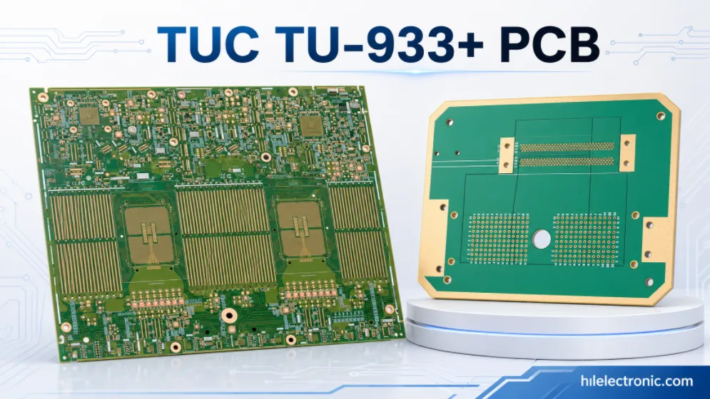
TUC TU-933+ PCB refers to a high-speed or RF printed circuit board fabricated with the ThunderClad 3+ material system—TU-933+ laminate and TU-933P+ prepreg. TUC manufactures the base material. Highleap Electronics does not manufacture the laminate; we manufacture the PCB and assemble the PCBA.
TUC publicly positions TU-933+ as a super-low-loss, high-thermal-reliability material for high-performance computing, telecom, backplanes, servers and RF applications. Highleap uses the customer-approved material construction as one part of a complete channel and manufacturing release.
Can Highleap manufacture a TU-933+ PCB? Yes, after confirming the exact TU-933+/TU-933P+ constructions, copper profile, stackup, impedance, channel requirements and material availability. We support bare-board fabrication and turnkey or consigned PCB assembly.
What Is TU-933+ PCB Material?
TU-933+ is the laminate in TUC’s ThunderClad 3+ system; TU-933P+ is the related prepreg. TUC lists a representative dielectric constant of 3.08 and dissipation factor of 0.0020 at 10 GHz, together with stable Dk/Df behavior, moisture resistance, low Z-axis expansion, dimensional stability and CAF resistance.
A purchaser does not need to master every technical term in this section. What matters is that the files show the intended circuit and that the factory can identify the sensitive production variables. Highleap coordinates the review with the relevant specialists and explains the consequences in terms of feasibility, cost, lead time and acceptance.
From the factory side, the name describes an application class, not a complete purchase specification. A quotation becomes reliable only after the design has been connected to available material constructions, copper, holes, surface finish and test requirements. The assigned engineer handles that translation and returns only the unresolved choices that need customer approval.
Why TU-933+ Is Used in 112G-Class and High-Layer-Count PCBs
Lower channel loss
Low Df reduces dielectric loss, while low-profile copper and controlled routing reduce conductor loss. Both must be represented in the channel model.
High-layer-count compatibility
The thermoset system is designed for complex multilayers and modified FR-4 processing, making it relevant to dense server and switch architectures.
Thermal reliability
Lead-free assembly and rework require material stability, plated-hole integrity and moisture control across the complete PCB.
Dimensional control
Stable thickness and panel movement help registration, impedance and back-drill accuracy on large boards.
For buyers, the commercial consequence of selection is immediate: the decision changes sourcing, lead time, process capability and test scope. Choosing too little margin can produce loss mismatch caused by copper substitution or lamination defects in dense stackups; choosing far more margin than the channel needs increases cost without improving yield. Our assigned engineer explains that trade-off in project terms, not as a generic materials lecture.
Selection should start with the dominant product constraint. The requested solution is justified when it directly improves back-drilled or HDI via architecture, low-loss laminate and prepreg selection or low-profile copper; it is less useful when the real limitation is a connector, via transition, thermal path or assembly feature. This prevents premium material from being used as a substitute for correcting the actual channel or reliability problem.
Where TU-933+ PCBs Are Used
Typical projects include AI and HPC servers, switch and router line cards, storage platforms, high-speed backplanes, telecom base stations, RF subsystems and high-speed test fixtures. The correct material choice depends on total channel length and loss—not the product label alone.
Short channels
A less expensive low-loss material may meet the budget. Using TU-933+ without a measured need can add cost and procurement risk.
Long or connector-rich channels
TU-933+ becomes more valuable when insertion-loss analysis shows that dielectric and copper losses are consuming system margin.
The factory should also state when another construction may be more appropriate. Under-specification can leave excessive via stubs, insufficient loss margin or weak thermal reliability. Over-specification can increase material cost and sourcing time without correcting connector, breakout or return-path discontinuities. Highleap can compare manufacturable options, but the approved material and qualification basis remain under customer change control.
The practical outcome is a clear go/no-go decision: use the requested solution when the performance or compliance requirement needs it; choose a simpler approved construction when it does not. That judgement is made from the board and product data, not from the assumption that the highest specification always produces the best PCB.
Implications of Treating TU-933+ as a Simple FR-4 Upgrade
- Wrong copper profile: channel loss can miss simulation even when the resin system is correct.
- Uncontrolled glass style or resin content: impedance, skew and pressed thickness can vary.
- Long via stubs: resonance and return loss can dominate the material improvement.
- Back-drill misregistration: poor depth control can leave excessive stub or damage the target layer.
- Assembly warpage: large, high-layer-count boards need copper balance, support tooling and profile control.
- Unapproved substitution: a similar “super-low-loss” grade is not automatically equivalent.
These risks should lower the effort required to contact the factory, not raise it. Once Highleap receives the Gerber or design files, we check registration and plating control, coupon-based production release, approved construction traceability and pressed-thickness and impedance correlation. Only decisions that materially affect function, compliance, price or delivery are returned to the customer.
A broad response such as tightening every tolerance is usually wasteful. The correct action depends on whether the dominant cause is high-layer-count resin fill, back-drilled or HDI via architecture, low-loss laminate and prepreg selection or low-profile copper. Targeted controls improve yield and make the root cause traceable without turning the entire drawing into an unnecessarily expensive special process.
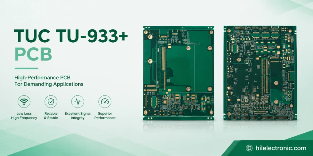
TU-933+ Stackup and Channel Planning
Highleap reviews the stackup as a signal-integrity and manufacturing system. The release should identify core/prepreg constructions, copper profile, glass style where controlled, finished copper, impedance, pair geometry, back drilling and coupon methodology.
| Channel variable | Manufacturing control | Customer input |
|---|---|---|
| Dielectric loss | Verified TU-933+ system and pressed thickness | Frequency range and loss target |
| Conductor loss | Approved low-profile copper and etch control | Copper model and finished copper |
| Skew | Glass construction, routing orientation and pair geometry | Maximum intra-pair skew |
| Via discontinuity | Via design, back-drill depth and inspection | Padstack and residual-stub target |
| Connector launch | Anti-pad, reference transition and local geometry | Connector model and compliance target |
The technical variables in this section cannot be evaluated independently. A change in back-drilled or HDI via architecture can alter the effect of low-loss laminate and prepreg selection, while low-profile copper and high-layer-count resin fill influence the geometry and test result seen on the finished board. Highleap reviews the actual production construction so the stackup and compensation are based on purchasable materials rather than nominal examples.
High-layer-count TU-933+ boards require enough resin to fill dense copper patterns while maintaining the dielectric thickness used in the channel model. Critical layer pairs should use the approved copper profile, and via stubs must be managed through HDI, blind vias or back drilling where justified. The stackup also needs balanced copper and practical press cycles so electrical performance does not create avoidable warpage or lamination risk.
Highleap TU-933+ PCB Manufacturing Capabilities
Highleap supports high-layer-count rigid boards, HDI structures, sequential lamination, via-in-pad, back drilling, controlled impedance and fine-line fabrication. Our published high-frequency platform includes impedance verification, AOI, electrical test, cross-section inspection and optional S-parameter or insertion-loss testing for critical channels.
Feasibility limits depend on board size, total thickness, copper distribution, layer count and the selected TU-933+ construction. A generic capability number is not a substitute for project DFM.
Manufacturing feedback is presented as specific actions. Routine CAM and process decisions stay with Highleap; questions are sent to the customer only when they change function, qualification, cost or lead time. That service model keeps complex fabrication from becoming an administrative burden for purchasing.
The approved manufacturing data are retained for repeat orders. Material identity, scaling, drill route, plating target and inspection method remain under change control. This protects the product from lamination defects in dense stackups or back-drill or via-stub errors caused by an undocumented process or supply change.
TU-933+ PCB Assembly for Servers, Switches and Telecom Hardware
High-speed board performance can be damaged during assembly by warpage, connector misalignment, BGA voiding, excessive rework or contamination. Highleap provides stencil engineering, SPI, SMT placement, controlled reflow, AOI, X-ray, press-fit or through-hole processing and functional testing when fixtures and procedures are supplied.
For large backplanes and line cards, assembly review includes support tooling, heavy-connector insertion, BGA escape inspection, thermal mass and rework limits.
The assembly process begins with the bare-board construction. Warpage, copper balance, pad finish, via condition and thermal mass influence printing, placement and reflow. Highleap reviews the PCB and component layout together so a board that meets bare-board tests does not become a low-yield PCBA after high-value parts are loaded.
Inspection is selected by package and defect risk. SPI controls paste deposition, AOI checks visible placement and solder features, and X-ray is used where joints are hidden. Special optical, RF or mechanical interfaces may also require fixtures, datum checks or customer handling instructions.
Send the Board Files First for a TU-933+ PCB Quote
Start by sending the Gerber files or native PCB design files. You do not need to organize a separate list of stackup, copper, back-drill and loss requirements before speaking with us. When those notes are already inside the design package, we use them directly.
One engineer coordinates the technical review
Your dedicated Highleap engineer will work with you one to one and review the high-speed layers, TU-933+ construction, impedance, back drilling and assembly needs with our specialist engineering team. We will explain any issue in practical terms and request only the files needed for the next step. If PCBA is required, the BOM and placement data can follow after the PCB review has started.
The assigned engineer keeps all communication in one project path. Material, stackup, CAM, fabrication, quality and assembly questions are consolidated so the buyer does not have to route technical issues between multiple factory departments.
TU-933+ PCB Price and Lead-Time Drivers
Primary cost drivers are material lead time, high layer count, panel utilization, sequential lamination, low-profile copper, tight impedance, back drilling, coupon space, test scope and yield risk. PCBA cost depends on BGA count, connector processing, component availability, inspection depth and functional test.
Highleap confirms current material supply and does not promise a fixed lead time before reviewing the exact construction.
Lead time is often controlled by material availability, special copper, supplier minimums, sequential processing or outside characterization. The engineer identifies the actual schedule constraint and checks whether an approved alternative can remove it without changing the product requirement.
Cost reduction should remove unnecessary complexity, not the control that protects performance. Highleap reviews panel utilization, noncritical layer construction, via architecture and test scope. Any proposal that changes approved material, copper, stackup or qualification is returned for customer approval.
The exact laminate, prepreg and copper construction can have a larger schedule impact than the board outline. High layer count, large panel size, multiple lamination cycles, back drilling and loss coupons add process time and reduce panel yield. Highleap can compare approved constructions and identify where complexity is supporting the channel requirement and where it can be removed without weakening the design.
High-Speed Performance Requires a Controlled Production Release
TU-933+ can preserve channel margin, but only when material, copper, glass, stackup, vias, connectors and assembly are controlled as one system. Highleap Electronics provides the fabrication, assembly and test path; TUC remains the material manufacturer.
A coupon must represent the feature being controlled. Layer pair, copper, dielectric thickness, routing geometry and panel position should correspond to the critical circuit. Our engineers confirm whether a standard impedance coupon is sufficient or whether a dedicated loss, resonator or customer test structure is needed.
Standard electrical test verifies opens and shorts, but it does not prove every performance requirement. Depending on the design, the plan may also use impedance, microsection, back-drill verification, optional insertion-loss coupons and PCBA inspection. Highleap distinguishes production verification from full product qualification so the quoted test scope matches the decision the result is expected to support.
Frequently Asked Questions
Is TU-933+ the same as TU-933?
No. The exact grade and related prepreg must be specified. Similar names do not authorize substitution.
Does Highleap manufacture TU-933+ laminate?
No. TUC manufactures the laminate and prepreg. Highleap manufactures PCBs and PCB assemblies using the approved material.
Is TU-933+ suitable for 112G PCB channels?
It can be suitable, but selection must be based on the complete channel loss, reach, copper, vias and connector architecture.
Do I need a finished stackup and back-drill table before contacting Highleap?
No. Send the Gerber files or PCB design files first. A Highleap engineer will review the board one to one and confirm the stackup, copper, impedance and back-drill details with the engineering team.
Can you assemble high-layer-count TU-933+ boards?
Yes. We support SMT, BGA, through-hole, press-fit, AOI, X-ray and functional test based on the assembly package.
Who helps confirm the missing TU-933+ manufacturing details?
A dedicated Highleap engineer works with you directly and coordinates the stackup, copper, impedance, back drilling, fabrication and assembly review with our specialist engineering team.
Technical reference note: Material properties and interface descriptions must be checked against the current manufacturer datasheet, customer specification and applicable interface standard for the exact production construction. Highleap Electronics is the PCB fabrication and PCB assembly provider; laminate and component trademarks belong to their respective manufacturers.

Recommended Posts
TMM6 Filter PCB Manufacturing
Table of contentsWhy Microwave Filter Designers Use...

TMM4 Filter PCB Manufacturing
TMM4 filter PCB manufacturing is controlled by the...

TMM3 PCB Manufacturing for RF Modules
TMM3 PCB manufacturing is most useful where the RF module...

TMM6 PCB Fabrication
TMM6 fabrication is the process-control page for a mid-Dk...
How to get a quote for PCBs
Let’s run DFM/DFA analysis for you and get back to you with a report. You can upload your files securely through our website. We require the following information in order to give you a quote:
-
- Gerber, ODB++, or .pcb, spec.
- BOM list if you require assembly
- Quantity
- Turn time
For PCBA services, please provide your BOM (Bill of Materials) and any specific assembly instructions. We also offer DFM/DFA analysis to optimize your designs for manufacturability and assembly, ensuring a smooth production process.