
PCB Glass Weave Effect: Design, Material and Manufacturing Control
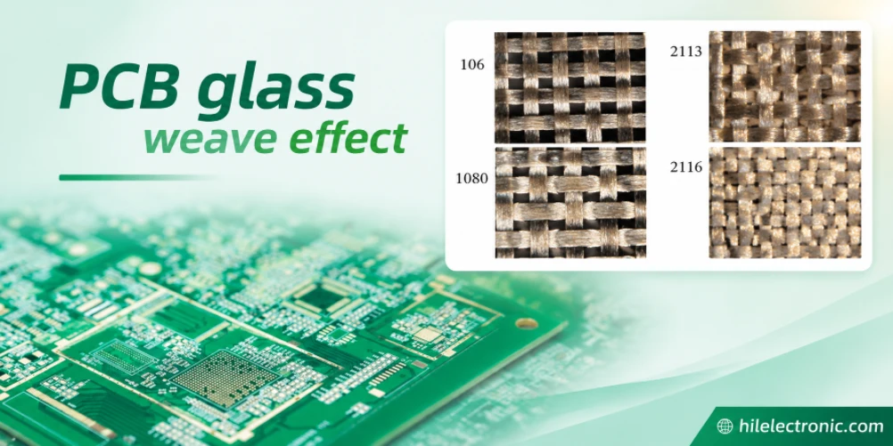
PCB glass weave effect occurs because woven glass and resin have different dielectric properties. A trace or differential pair can sample different proportions of glass and resin, producing local differences in effective Dk, delay and impedance.
Highleap Electronics does not manufacture glass cloth or laminate. We manufacture PCBs and PCBAs using customer-approved constructions, and we help control glass style, stackup, panel orientation, routing assumptions and test coupons.
Does glass weave effect matter on every PCB? No. It becomes important when data rate, differential length, pair geometry, dielectric thickness and glass pattern create meaningful skew, jitter or resonant behavior. The risk should be evaluated, not assumed or ignored.
What Causes PCB Glass Weave Effect?
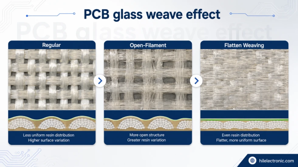
PCB dielectric layers are composite structures. Glass bundles typically have a higher Dk than the surrounding resin. When one conductor sits over more glass and the other over more resin, their propagation delays can differ. Periodic glass patterns can also produce impedance variation and resonances.
Across a differential pair
Different local Dk can create intra-pair skew and mode conversion.
Along a trace
Periodic dielectric loading can create resonant features in insertion or return loss.
Between production lots
Glass style, resin content and construction changes can move the electrical result.
Between routing angles
Trace angle changes how often conductors cross glass bundles and resin windows.
Repeatability is the main manufacturing test. A prototype can work even when the process window is broad, but volume production exposes variation in material lots, copper distribution, panel loading and plating. We place routing and stackup review, material construction traceability, representative skew or loss coupon planning and glass-style confirmation in the production release to provide a stable comparison between lots.
When Glass Weave Effect Becomes a Design Risk
- Long differential pairs at high data rates.
- Thin dielectric layers where traces strongly sample local glass/resin variation.
- Loose differential coupling that allows each trace to experience a different dielectric region.
- Open-weave glass styles with larger resin windows.
- Channels with very small skew or jitter margin.
- High-frequency resonant or phase-matched structures.
A headline data rate is not enough. Pair length, rise time, coupling, glass pitch and routing direction determine the practical risk.
Repeatability is the main manufacturing test. A prototype can work even when the process window is broad, but volume production exposes variation in material lots, copper distribution, panel loading and plating. We place representative skew or loss coupon planning, glass-style confirmation, routing and stackup review and material construction traceability in the production release to provide a stable comparison between lots.
The risk increases when a differential pair is long enough for the two traces to sample different glass-and-resin regions, when the dielectric is thin, or when timing margin is already small. Short local routes may not justify a premium spread-glass construction. The decision should therefore use route length, pair orientation, glass style, resin content and the allowed skew rather than applying the same rule to every high-speed PCB.
Electrical Symptoms of Glass Weave Effect
| Symptom | Possible mechanism | How to investigate |
|---|---|---|
| Intra-pair skew | Different effective Dk under each conductor | TDR/TDT, phase delay and construction review |
| Mode conversion | Differential imbalance | Mixed-mode S-parameters |
| Insertion-loss ripple | Periodic dielectric loading | Frequency-domain coupon measurement |
| Impedance variation | Local field distribution changes | Field modeling and TDR |
| Lot-to-lot timing change | Construction or resin variation | Material traceability and coupon correlation |
Generic datasheet values are not enough when ordinary electrical testing cannot detect lane-to-lane or pair-to-pair skew or eye closure that is difficult to reproduce. The review must use the exact core or prepreg, copper profile, finished thickness and via route. This is where one-to-one engineering support prevents the buyer from having to interpret multiple supplier documents alone.
Generic datasheet values are not enough when ordinary electrical testing cannot detect different results between prototype lots or false confidence from using only a bulk Dk value. The review must use the exact core or prepreg, copper profile, finished thickness and via route. This is where one-to-one engineering support prevents the buyer from having to interpret multiple supplier documents alone.
How Designers Mitigate Glass Weave Effect
- Use spread or tighter-weave glass: reduces large resin-rich windows.
- Consider low-Dk glass: reduces the Dk contrast between glass and resin.
- Route at a controlled angle: can average local variation, but the angle should be checked against possible periodic resonances.
- Increase differential coupling: a more tightly coupled pair can reduce sensitivity to local asymmetry.
- Choose trace placement deliberately: broadside and edge-coupled structures respond differently.
- Include skew in the channel budget: deskew features should not replace basic stackup control.
Rotating traces by an arbitrary angle is not a universal cure. Trace length, glass pitch and target bandwidth should be considered.
The technical variables in this section cannot be evaluated independently. A change in local glass and resin distribution can alter the effect of differential-pair orientation, while spread-glass construction and pressed dielectric thickness influence the geometry and test result seen on the finished board. Highleap reviews the actual production construction so the stackup and compensation are based on purchasable materials rather than nominal examples.
Mitigation methods have different costs and limitations. Rotating routes can reduce repeated alignment with the weave but may complicate placement and panelization. Wider traces or closer pair spacing change impedance and crosstalk. Spread-glass materials reduce local inhomogeneity but can narrow the approved supply options. Highleap reviews these choices against the production stackup so the selected method remains manufacturable and repeatable.
How PCB Manufacturing Affects Glass Weave Control
The manufacturer controls which purchasable core/prepreg constructions are used, how panels are oriented, how dielectric thickness is pressed and how stackup changes are managed. A fabrication note that says only “low-loss material” does not control glass weave.
Highleap production controls
- verify exact glass style and resin content when specified;
- maintain approved stackup and material traceability;
- control panel orientation where routing angle depends on warp/fill direction;
- measure final thickness and impedance;
- build representative coupons for skew or S-parameter testing when required.
Different designs require different process windows. Board thickness, material chemistry, copper balance, hole architecture and panel size can change preparation, pressing and plating conditions. The assigned engineer coordinates CAM, production and quality so the customer receives one manufacturing answer instead of separate questions from each department.
A capability claim has value only when it is connected to a controlled shop-floor route. Highleap links material construction traceability, representative skew or loss coupon planning, glass-style confirmation and routing and stackup review to incoming inspection, lamination, drilling, plating, imaging and final verification. The exact sequence remains subject to the approved material and board construction.
Implications of Ignoring the Weave in Procurement
- A “same Dk/Df” substitute can use a different glass construction.
- Moving production between regions can change available glass styles.
- Prepreg resin content changes can alter the dielectric mix and pressed thickness.
- Panel rotation during CAM can invalidate a routing-angle mitigation strategy.
- Using only average bulk Dk can hide local differential imbalance.
Repeat production creates another risk: a later lot can use a different available construction while the nominal material family remains unchanged. Highleap records the approved stackup, copper, process assumptions and inspection method so prototypes and production are compared against the same release basis.
A broad response such as tightening every tolerance is usually wasteful. The correct action depends on whether the dominant cause is pressed dielectric thickness, local glass and resin distribution, differential-pair orientation or spread-glass construction. Targeted controls improve yield and make the root cause traceable without turning the entire drawing into an unnecessarily expensive special process.
Highleap High-Speed PCB and PCBA Support
Highleap supports controlled stackups, low-loss materials, low-Dk glass constructions, controlled impedance, HDI, back drilling, fine-line fabrication and optional high-speed coupon testing. For assembly, we control warpage, fine-pitch placement, connector insertion and inspection so the fabricated channel is not degraded during PCBA.
This subject becomes useful when it is converted into a production decision. Highleap checks spread-glass construction, pressed dielectric thickness, local glass and resin distribution and differential-pair orientation, then records the agreed result in the stackup, process route and inspection plan. Purchasing receives a clear feasibility and quotation response rather than a theoretical explanation alone.
Most of the initial information is already present in the Gerber or PCB design files. Our engineer identifies any unresolved point, coordinates our signal-integrity, material, CAM and fabrication engineers and asks the customer only for decisions that affect function, qualification, cost or schedule.
Send the PCB Files; Our Engineer Will Check the Weave Risk
You do not need to prepare a special glass-weave questionnaire. Send the Gerber files or PCB design files first. Existing stackup or fabrication notes can remain in the design package; there is no need to duplicate them.
Highleap turns the design into practical production controls
A dedicated Highleap engineer will work with you one to one and review the differential routing, layer construction and expected data rate with our high-speed PCB team. We will determine whether glass style, panel orientation, routing angle or additional coupon control needs to be discussed. Only the missing decisions will be brought back to you.
The first quotation step is intentionally simple: send the Gerber files or native PCB design files. If fabrication notes and stackup information are already included, they do not need to be copied into another form. A dedicated Highleap engineer reviews the data and coordinates the necessary specialists.
Cost of Glass-Weave Mitigation
Spread glass, low-Dk glass, controlled constructions, orientation constraints and specialized test coupons can increase material cost or reduce panel utilization. The correct decision is based on measured risk. Over-specifying glass style on every layer can add cost without improving the channel.
Two boards with the same size and layer count can therefore have different prices. The relevant comparison is not unit material cost alone, but the manufacturing route, inspection burden, expected yield and amount of engineering or qualification work required for release.
Yield must be considered from prototype through volume. Features associated with different results between prototype lots or lane-to-lane or pair-to-pair skew can increase scrap, rework and component loss. A stable documented construction usually has a lower total cost than an aggressive design that needs repeated changes after assembly.
Control the Construction, Not Only the Material Family
Glass weave effect is a system-level interaction between dielectric construction and trace geometry. Highleap helps customers convert the mitigation strategy into a released stackup, panel orientation and test plan.
Repeatability is the main manufacturing test. A prototype can work even when the process window is broad, but volume production exposes variation in material lots, copper distribution, panel loading and plating. We place material construction traceability, representative skew or loss coupon planning, glass-style confirmation and routing and stackup review in the production release to provide a stable comparison between lots.
Generic datasheet values are not enough when ordinary electrical testing cannot detect eye closure that is difficult to reproduce or different results between prototype lots. The review must use the exact core or prepreg, copper profile, finished thickness and via route. This is where one-to-one engineering support prevents the buyer from having to interpret multiple supplier documents alone.
Frequently Asked Questions
Is PCB glass weave effect the same as dielectric loss?
No. It is primarily an inhomogeneity effect that can cause skew, mode conversion, impedance variation and resonances.
Does rotating differential pairs always solve the problem?
No. Rotation can help average the dielectric, but angle, trace length, glass pitch and bandwidth must be checked.
What is spread glass?
A glass fabric construction with more uniform fiber distribution and smaller resin-rich windows than an open weave.
Can the PCB factory guarantee zero weave skew?
No realistic factory should guarantee zero. The risk can be reduced and verified against defined limits using controlled construction and coupons.
Does Highleap manufacture glass fabric?
No. We manufacture PCBs using specified laminates and control the production construction.
What should I send Highleap if I am concerned about glass weave effect?
Send the Gerber files or native PCB design files first. Our engineer will review the routing and stackup with the high-speed PCB team and ask only for any missing performance limits or material decisions.
Technical reference note: Material properties and interface descriptions must be checked against the current manufacturer datasheet, customer specification and applicable interface standard for the exact production construction. Highleap Electronics is the PCB fabrication and PCB assembly provider; laminate and component trademarks belong to their respective manufacturers.

Recommended Posts

TMM4 Filter PCB Manufacturing
TMM4 filter PCB manufacturing is controlled by the...

TMM3 PCB Manufacturing for RF Modules
TMM3 PCB manufacturing is most useful where the RF module...

TMM6 PCB Fabrication
TMM6 fabrication is the process-control page for a mid-Dk...

TMM10 PCB Manufacturing for Compact RF Designs
Table of contentsHow TMM10 Shrinks RF StructuresTMM10 vs...
How to get a quote for PCBs
Let’s run DFM/DFA analysis for you and get back to you with a report. You can upload your files securely through our website. We require the following information in order to give you a quote:
-
- Gerber, ODB++, or .pcb, spec.
- BOM list if you require assembly
- Quantity
- Turn time
For PCBA services, please provide your BOM (Bill of Materials) and any specific assembly instructions. We also offer DFM/DFA analysis to optimize your designs for manufacturability and assembly, ensuring a smooth production process.