
Shengyi S7136H Leiterplattenfertigung und Bestückungsservice
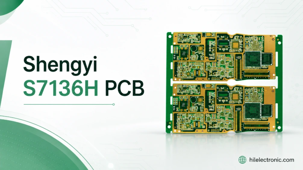
A Shengyi S7136H PCB is a printed circuit board fabricated with verified S7136H high-frequency laminate in the RF-critical layers. Shengyi manufactures the laminate. Highleap Electronics manufactures the PCB and provides PCB assembly; we do not manufacture S7136H material.
We support prototype, low-volume and production builds subject to material availability and project-specific DFM approval. Our engineering review connects the selected S7136H construction to impedance, copper profile, drilling, lamination, surface finish, assembly and acceptance testing.
Can Highleap build your S7136H PCB? Yes, when the exact laminate construction, copper, stackup and electrical requirements are available for review. Send Gerber or ODB++, fabrication drawing, stackup, impedance table and quantity. For assembly, also send the BOM, centroid data and assembly drawings.
What Is a Shengyi S7136H PCB?
S7136H is a glass-reinforced hydrocarbon-and-ceramic high-frequency laminate. The material manufacturer positions it for low-loss RF and microwave circuits requiring stable electrical properties over frequency, low Z-axis expansion and dimensional stability.
What the material contributes
- Low-loss dielectric behavior for RF transmission lines.
- Controlled dielectric properties for repeatable impedance and phase.
- Dimensional stability for antennas, filters and multilayer registration.
- Compatibility with lead-free assembly when the complete board is properly qualified.
What the PCB factory must control
- Actual core thickness, copper type and finished copper.
- Artwork compensation and RF-critical line geometry.
- Drilling, hole-wall quality, plating and multilayer registration.
- Surface finish, solder mask and final inspection criteria.
The material name alone does not define the finished PCB. Two boards both called “S7136H PCB” can perform differently if they use different core thicknesses, copper profiles, line widths, surface finishes or stackups.
Die Definition wird dann wirtschaftlich relevant, wenn sie die Frage beantwortet, ob das Design herstellbar ist und welche Parameter vom Prototyp bis zur Serienfertigung unverändert bleiben müssen. Materialart, Leiteraufbau, vertikale Verbindungen und mechanische Referenzen können das Ergebnis beeinflussen. Unsere Ingenieure trennen zwingende Leistungsbedingungen von Präferenzen und dokumentieren anschließend die für Nachbestellungen erforderlichen Fertigungskontrollen.
The term describes a PCB fabricated with a customer-approved Shengyi S7136H material construction; it does not mean Highleap manufactures the laminate. The exact core, prepreg, copper and thickness must still be identified in the production stackup. Highleap purchases the approved material, processes it into the PCB, and provides assembly and testing when required.
Why Designers Choose S7136H for RF and Microwave Circuits
S7136H is normally selected when ordinary FR-4 creates too much loss or insufficient dielectric control, but the project still needs a practical manufacturing route for antennas, RF modules and hybrid multilayers.
Electrical advantages
Stable dielectric behavior helps preserve impedance, phase length and resonant frequency. Low dielectric loss reduces attenuation along RF traces, although total loss still includes copper roughness, conductor geometry, launches, vias and connectors.
Mechanical and production advantages
Glass reinforcement and low Z-axis expansion can support dimensional stability and plated-hole reliability. These characteristics are useful in larger RF panels and multilayer structures where registration and thermal cycling matter.
When another material may be better
S7136H is not automatically the best choice for every high-frequency design. Very low-Dk antenna structures, extreme mmWave loss budgets, unusual temperature-coefficient requirements or an already-qualified legacy stackup may justify another laminate. Highleap reviews the electrical target and the complete construction rather than recommending a material only by brand name.
Application lists are not proof of suitability. Two products in the same market can have different layer counts, trace lengths, operating environments and test limits. Our review therefore links the product use to Dk and Df basis, copper profile, impedance and thermal requirements and approved S7136H core and prepreg constructions before confirming that the requested construction is the right commercial choice.
Applications of S7136H PCBs
Base-station antennas
Controlled dielectric properties and repeatable thickness support antenna feeds, phase networks and matching structures.
Leistungsverstärker
Low-loss RF routing and thermal planning are important around power devices, matching networks and grounded structures.
Automotive and phased-array radar
Fine geometry, phase matching and consistent dielectric construction must be controlled together.
LNA, LNB and satellite equipment
Low-noise signal paths benefit from controlled loss, clean assembly and stable RF launches.
For buyers, the commercial consequence of selection is immediate: the decision changes sourcing, lead time, process capability and test scope. Choosing too little margin can produce impedance drift from thickness or copper changes or unplanned loss from rougher foil; choosing far more margin than the channel needs increases cost without improving yield. Our assigned engineer explains that trade-off in project terms, not as a generic materials lecture.
Eine sorgfältige Auswahl berücksichtigt auch die Lieferkontinuität. Kernstärke, Prepreg, Kupferprofil und Zertifikate sind möglicherweise nicht alle mit der gleichen Lieferzeit verfügbar. Highleap prüft die genaue Konstruktion und identifiziert etwaige Lieferrisiken vor der Werkzeugfertigung, anstatt nach Freigabe des Designs eine vergleichbare Sorte zu verwenden.
What Happens If the Material or Stackup Is Chosen Incorrectly?
- Impedance moves out of tolerance: using a generic Dk or an unapproved thickness changes line geometry and effective impedance.
- Filters and antennas shift: resonant structures can move in frequency when dielectric thickness, Dk or etch geometry changes.
- Insertion loss exceeds the budget: rough copper, long paths, unsuitable finish or poor launches can consume the benefit of the laminate.
- Hybrid boards warp or delaminate: incompatible materials, resin systems and press cycles can create stress and registration errors.
- Assembly damages the board: moisture, reflow history, heavy components and local thermal mass must be considered in the PCBA plan.
Bei der Nachbearbeitung besteht ein weiteres Risiko: Eine spätere Charge kann eine andere verfügbare Konstruktion verwenden, während die nominelle Materialfamilie unverändert bleibt. Highleap erfasst den freigegebenen Schichtaufbau, die Kupferbelegung, die Prozessannahmen und die Prüfmethode, sodass Prototypen und Serienprodukte anhand derselben Freigabegrundlage verglichen werden.
The resulting board may still pass open-and-short testing while missing the intended RF or impedance behavior. Incorrect dielectric thickness, copper profile or Dk basis can change line width, phase length and insertion loss. If an unapproved substitute is introduced, material qualification and repeatability are also affected. The risk should be resolved during DFM, before components and test time are committed.
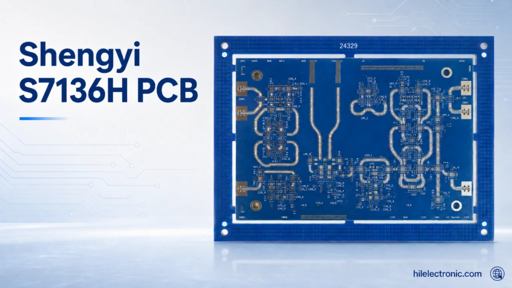
S7136H PCB Stackup and Design Requirements
Before tooling, Highleap confirms the released material construction and calculates the production geometry from the agreed stackup. RF-critical dimensions should be identified separately from ordinary digital or mechanical dimensions.
| Design-Eingabe | Warum es wichtig ist | What Highleap reviews |
|---|---|---|
| Core and prepreg callout | Defines dielectric system and availability | Exact grade, thickness, copper and approved alternatives |
| Impedance and frequency | Controls line width, spacing and test method | Field-solver model, coupon design and tolerance |
| RF-critical geometry | Filters, antennas and couplers are geometry-sensitive | Artwork compensation and inspection plan |
| Via and grounding strategy | Affects return current, inductance and shielding | Drill size, aspect ratio, via fence and plating |
| Oberflächenbeschaffenheit und Lötstoppmaske | Can affect loss, solderability and local dielectric loading | Finish selection and mask openings on critical structures |
Repeatability is the main manufacturing test. A prototype can work even when the process window is broad, but volume production exposes variation in material lots, copper distribution, panel loading and plating. We place material identity and lot traceability, stackup and artwork compensation, drilling, plating and lamination control and electrical and dimensional inspection in the production release to provide a stable comparison between lots.
A useful stackup identifies the exact S7136H construction, finished dielectric thickness, copper type, finished copper, impedance layers and bonding system. Hybride Designs also need agreement on how S7136H interfaces with FR-4 or another material during pressing. Highleap checks resin fill, copper balance, drill route and registration so the electrical model can be translated into a stable multilayer build.
Highleap S7136H PCB Manufacturing and Assembly Advantages
Highleap bietet Hochfrequenz-Leiterplattenherstellung, hybrid multilayer construction, controlled impedance, back drilling, via-in-pad, edge plating and selected RF finishes. Published platform limits are not automatic guarantees for every S7136H build; board size, thickness, layer count and material construction must pass DFM.
For PCBA, we support SMT and through-hole assembly, RF connector installation, shielding, heat-sink integration, SPI, AOI, Röntgeninspektion and customer-defined functional testing. Component sourcing can be full turnkey or customer-consigned.
Ein Projektingenieur koordiniert die Fertigung und alle Fragen rund um die SMD-Bestückung. Dadurch wird ein häufiger Fehler vermieden, bei dem die Leiterplatte optimiert wird, ohne die Bestückung zu berücksichtigen, oder der Bestückungsplan Pad-, Verzugs- und Temperaturbedingungen voraussetzt, die die Leiterplattenkonstruktion nicht zuverlässig gewährleisten kann.
Die Inspektion wird anhand des Gehäuses und des Fehlerrisikos ausgewählt. SPI kontrolliert den Pastenauftrag, AOI prüft die sichtbare Platzierung und Lötstellen, und Röntgen wird bei verdeckten Lötstellen eingesetzt. Spezielle optische, HF- oder mechanische Schnittstellen können außerdem Vorrichtungen, Bezugspunktprüfungen oder kundenseitige Handhabungsanweisungen erfordern.
How Highleap Manufactures an S7136H PCB
- Materialprüfung: confirm supplier, grade, construction, copper and traceability requirements.
- Stackup and CAM release: finalize impedance geometry, scaling and test coupons.
- Drilling and hole preparation: apply qualified parameters for clean hole walls and stable registration.
- Metallization and imaging: plate holes, transfer patterns and control RF-critical etch dimensions.
- Lamination for multilayers: use an approved bonding system and press cycle for the complete hybrid stack.
- Surface finish and profiling: protect RF surfaces and control board-edge geometry.
- Inspektion und Prüfung: AOI, electrical test, impedance verification and optional RF test structures.
- Montage und Endkontrolle: SPI, placement, reflow, AOI/X-ray and functional test when specified.
Der Zweck dieses Abschnitts ist daher sowohl technischer als auch kommerzieller Natur: Es soll erläutert werden, warum das Problem von Bedeutung ist, gezeigt werden, wie Highleap es kontrolliert, und dem Käufer soll ein einfacher Weg aufgezeigt werden, mit den bereits verfügbaren Dateien mit der Überprüfung zu beginnen.
The process begins with material verification and stackup release, followed by imaging, drilling, hole preparation, plating, lamination where required, etching, solder mask, surface finish and final inspection. The precise route depends on whether the design is a simple rigid RF board, a multilayer construction or a hybrid build. Highleap records the approved material and process details so later production lots follow the same basis.
Inspection can include AOI, electrical test, finished-thickness measurement, impedance coupons, microsection and customer-defined RF testing. The test method is agreed before production because an open-and-short result alone cannot verify every microwave requirement. For assembled boards, SMT, X-ray and functional test are added according to the component and product needs.
Start Your S7136H PCB Quote with the Gerber Files
You do not need to prepare a long technical package before contacting Highleap. Send the Gerber files or the original PCB design files first. If the fabrication notes are already included in the Gerber package, there is no need to create a separate document.
A Highleap engineer will take it from there
A dedicated engineer will review the S7136H material callout, stackup, impedance, copper, surface finish and test needs with our engineering team. We will contact you one to one and ask only for information that is genuinely missing. For PCB assembly, the BOM and placement files can be added after the initial PCB review.
Unvollständige Anfangsdaten führen nicht automatisch zur Ablehnung des Angebots. Wir ermitteln, was bereits definiert ist, unterscheiden Präferenzen von zwingenden Anforderungen und erläutern, welche offene Frage tatsächlich ein Hindernis darstellt. Falls eine Bestückung erforderlich ist, können Stückliste und Bestückungsdateien nach Klärung des Umfangs der Leiterplatte bereitgestellt werden.
S7136H PCB Cost and Lead-Time Factors
Cost is driven by material procurement, panel utilization, layer count, hybrid lamination, controlled impedance, tight RF geometry, via structure, copper weight, finish, testing and order quantity. Assembly cost also depends on BOM risk, package mix, X-ray needs, RF connectors, shielding and functional-test coverage.
Material availability can dominate lead time. Highleap confirms current supply before committing a production schedule and will not silently substitute a similar laminate.
Kostensenkungen sollten unnötige Komplexität beseitigen, nicht die Kontrolle, die die Leistung sichert. Highleap prüft die Panelauslastung, den Aufbau nichtkritischer Schichten, die Via-Architektur und den Testumfang. Jeder Vorschlag, der genehmigtes Material, Kupfer, Stackup oder die Qualifizierung ändert, wird dem Kunden zur Genehmigung vorgelegt.
Material availability and the exact construction often control the schedule. A common thickness and copper may be sourced more quickly than a special core, prepreg or foil combination. Hybrid lamination, tight impedance, small RF features and dedicated coupons also affect yield and inspection time. Highleap quotes from the submitted files and identifies the actual cost driver instead of applying one generic S7136H price.
Choose a PCB Manufacturer, Not Only a Material Name
S7136H can provide a strong RF platform, but the finished result depends on stackup discipline, copper control, etch accuracy, plated-hole quality, assembly and test. Highleap Electronics converts the customer-approved material specification into a manufacturable PCB and PCBA release.
Das Ergebnis der Überprüfung sollte ein realisierbarer Schichtaufbau und eine kurze Liste der kontrollierbaren Variablen sein. Highleap dokumentiert die vereinbarte Materialidentität, Geometrie, den Prozessablauf und die Prüfgrundlagen und koordiniert anschließend die verbleibenden Details intern mit den Bereichen CAM, Fertigung, Qualitätssicherung und Montage.
The technical variables in this section cannot be evaluated independently. A change in impedance and thermal requirements can alter the effect of approved S7136H core and prepreg constructions, while Dk and Df basis and copper profile influence the geometry and test result seen on the finished board. Highleap reviews the actual production construction so the stackup and compensation are based on purchasable materials rather than nominal examples.
Häufig gestellte Fragen
Does Highleap manufacture Shengyi S7136H material?
No. Shengyi manufactures the laminate. Highleap Electronics procures or processes verified customer-specified material and manufactures the PCB and PCBA.
Can Highleap build multilayer or hybrid S7136H PCBs?
Yes, subject to stackup, bonding-material compatibility, material availability and DFM approval.
What should I send first for an S7136H PCB quote?
Send the Gerber files or native PCB design files. If fabrication notes are already included, that is enough to begin. A Highleap engineer will review the design one to one and request only the missing details.
Do you offer S7136H PCB assembly?
Yes. Highleap supports component sourcing, SMT, through-hole assembly, RF connectors, shielding, AOI, X-ray and functional testing as required.
Will a Highleap engineer contact me after I upload the files?
Yes. A dedicated engineer will review the Gerber or PCB design files, contact you one to one, and coordinate any material, stackup, impedance, testing or assembly questions with the appropriate Highleap engineering team.
Can S7136H be replaced with another RF material?
Only after electrical, mechanical, thermal, supply and qualification review. No substitution should be made from Dk alone.
Technischer Referenzhinweis: Die Materialeigenschaften und Schnittstellenbeschreibungen müssen anhand des aktuellen Herstellerdatenblatts, der Kundenspezifikation und der geltenden Schnittstellennorm für die jeweilige Fertigungsausführung überprüft werden. Highleap Electronics ist der Anbieter für die Leiterplattenfertigung und -bestückung; Laminat- und Bauteilmarken gehören den jeweiligen Herstellern.

Empfohlen Beiträge

Taconic RF-35 Leiterplattenfertigungsservice – Prototypenentwicklung bis Serienproduktion
Abbildung 1. Taconic RF-35 Leiterplatte. Die Taconic RF-35 ist das Arbeitspferd...

Isola Astra MT77 Leiterplattenfertigung
Abbildung 1. Isola Astra MT77 LeiterplattenfertigungIsola Astra...

Kundenspezifische Rogers RO4835 Leiterplattenfertigung & -bestückung
Abbildung 1. Rogers RO4835 Leiterplatte. Die Rogers RO4835 Leiterplatte ist eine...

Nelco N4000-13 Leiterplattenmaterial- und Fertigungsleitfaden | Highleap Electronics
Abbildung 1. Nelco N4000-13 Leiterplatte. Die Nelco N4000-13 Leiterplatte ist eine...
So erhalten Sie ein Angebot für Leiterplatten
Wir führen gerne eine DFM/DFA-Analyse für Sie durch und senden Ihnen anschließend einen Bericht zu. Sie können Ihre Dateien sicher über unsere Website hochladen. Für die Erstellung eines Angebots benötigen wir folgende Informationen:
-
- Gerber, ODB++ oder .pcb, Spezifikation.
- Stückliste, wenn Sie eine Montage benötigen
- Die Menge
- Wendezeit
Für PCBA-Dienstleistungen geben Sie bitte Ihre Stückliste (BOM) und alle spezifischen Montageanweisungen an. Wir bieten auch DFM/DFA-Analysen an, um Ihre Designs hinsichtlich Herstellbarkeit und Montage zu optimieren und so einen reibungslosen Produktionsprozess zu gewährleisten.